
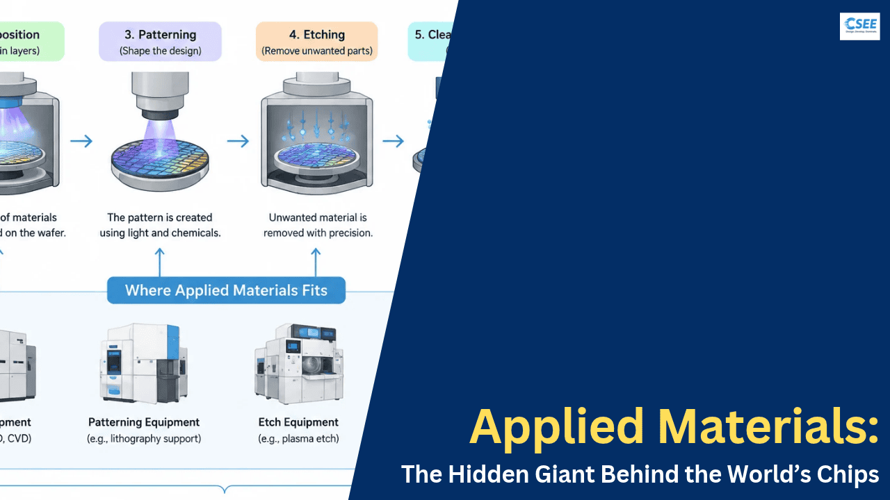
Applied Materials: The Machines Behind Every Chip
Ask people who makes the world’s chips and they name NVIDIA, Apple, Intel, or TSMC. Far fewer name Applied Materials, a company that builds the machines those chipmakers depend on to turn silicon discs into working processors and memory.
The company you never see on the box
A chip designer such as NVIDIA or Apple draws a circuit. A foundry such as TSMC or Samsung builds it. But neither can build anything without equipment: furnaces, vacuum chambers, plasma etchers, polishers and microscopes that operate with atomic precision. Applied Materials, based in Santa Clara, California, is one of the largest suppliers of that equipment, and it sits next to rivals such as ASML, Lam Research, Tokyo Electron and KLA in what the industry calls the wafer fab equipment ecosystem.
The simplest way to understand the company is by analogy. If a chip is a skyscraper built from a thousand microscopic floors, the designers are the architects, the foundries are the construction firms, and Applied Materials makes many of the cranes, concrete mixers, welding rigs and inspection tools. The building cannot rise without them.
How a chip is actually made
A chip starts as a thin disc of ultra-pure silicon called a wafer. Hundreds of copies of a chip are built on it at once, layer by layer. The same family of operations repeats dozens of times, which is why equipment makers sell so many different machines to the same customer.
The major technology families
Deposition: adding layers
Deposition lays down films of metal, insulator or semiconductor, some only a few atoms thick. Several methods exist, and the choice depends on the material and the shape of the surface.
- Physical vapor deposition (PVD) knocks atoms off a solid target in a vacuum so they land on the wafer. It is common for metal films and liners.
- Chemical vapor deposition (CVD) uses reactive gases that form a solid film on the wafer surface.
- Atomic layer deposition (ALD) builds a film one atomic layer at a time, giving extreme uniformity inside deep, narrow structures.
- Epitaxy grows new crystalline silicon or silicon-germanium on the wafer, which is essential for modern transistors.
Etch: removing material
After a pattern is printed, etch tools remove material using plasma or chemistry, leaving only the intended shapes. As structures became tall and narrow, etching a clean, straight, deep channel became one of the hardest problems in the factory. Selective removal, which strips one material without touching its neighbor, is increasingly important.
Ion implantation: tuning the silicon
Implanters shoot charged atoms into silicon to change its electrical behavior. This is how regions are made to conduct more or less, forming the heart of every transistor.
Chemical mechanical planarization (CMP): making it flat
Each layer must be perfectly flat before the next is added. CMP polishes the wafer with a slurry and pad until the surface is smooth at nanometer scale. Without it, tall stacks of layers would not line up.
Inspection and metrology: checking the work
A single stray particle can kill a chip. Inspection tools, including electron-beam systems, hunt for defects, and metrology tools measure thicknesses and shapes. The data feeds back into the factory so that problems are caught early, which is vital when a wafer can be worth many thousands of dollars before it is finished.
Process steps and the tools behind them
| Step | What it does | Why it is hard |
|---|---|---|
| Deposition | Adds thin films of metal or insulator | Films must be uniform and only atoms thick |
| Epitaxy | Grows crystal layers on silicon | Crystal defects ruin transistors |
| Etch | Removes material to form shapes | Deep, narrow, straight cuts |
| Ion implant | Changes silicon conductivity | Precise dose and depth |
| CMP | Polishes surfaces flat | Nanometer-level flatness |
| Inspection | Finds defects and measures features | Defects are tiny and rare |
Why new chips need new materials
For decades chips improved by shrinking. Now shrinking alone is not enough, so the industry changes the structure and materials of the chip, and each change creates demand for new equipment. Applied Materials has spoken often about this shift, sometimes described as a move from simple scaling to a more materials-driven era.
From flat to three-dimensional transistors
Early transistors were flat. Around 2011 the industry adopted FinFETs, where the channel stands up like a fin and the gate wraps around it. The next step is gate-all-around (GAA) transistors, in which stacked ribbons of silicon are surrounded by the gate on every side. Making GAA requires alternating epitaxial layers, precise selective etching and conformal ALD films, all of which are core equipment areas.
Wiring problems
As wires shrink, resistance rises and signals slow. Engineers explore new metals and liner materials, as well as moving power delivery to the back of the wafer, which is called backside power. That change introduces extra steps such as wafer thinning, bonding and new deposition work.
Memory and advanced packaging
Memory is moving upward too. 3D NAND stacks hundreds of layers, demanding very deep etches. High bandwidth memory (HBM) stacks DRAM chips and links them with vertical connections, serving AI accelerators. Packaging, once an afterthought, now uses wafer-scale processes where deposition, etch and inspection matter, opening new opportunities for equipment suppliers.
| Inflection | Change | Equipment effect |
|---|---|---|
| FinFET | Vertical fin channel | More epitaxy and etch precision |
| Gate-all-around | Stacked nanosheets | Selective etch, ALD, epitaxy grow |
| Backside power | Power wires under the transistor | Thinning, bonding, new films |
| 3D NAND | Hundreds of stacked layers | Deep etch and thick deposition |
| HBM and packaging | Stacked dies, vertical links | Wafer-level deposition, etch, inspection |
Who buys the machines
The customers are the world’s major chip manufacturers. Foundries such as TSMC and Samsung build chips for others, Intel builds both its own designs and for outside clients, and memory makers such as Samsung, SK hynix and Micron buy equipment for DRAM and NAND. Chipmakers usually buy from several suppliers at once, since no single company covers every step. A new factory can cost tens of billions of dollars, and a large share of that is spent on equipment.
Relationships are long. A tool is qualified into a manufacturing process, and once a chipmaker has tuned its recipe around it, switching is expensive and risky. That stickiness helps explain the stability of the equipment business over time.
Where Applied Materials fits among equipment makers
| Company | Best known for |
|---|---|
| Applied Materials | Deposition, epitaxy, implant, CMP, e-beam inspection, broad portfolio |
| ASML | Lithography, including EUV, the only supplier of EUV systems |
| Lam Research | Etch and deposition, especially memory |
| Tokyo Electron | Coater/developers, etch, deposition, cleaning |
| KLA | Process control, inspection and metrology |
The overlap is real, but each company has a core strength. ASML prints the pattern, Lam and Tokyo Electron compete heavily in etch, KLA focuses on measurement, and Applied Materials is known for breadth across materials engineering.
How the business makes money
Revenue comes from selling new systems and from services: spare parts, upgrades, maintenance and software that keep installed machines productive for many years. Service revenue tends to be steadier than system sales, which rise and fall with the chip cycle. Because customers run tools for a decade or more, the installed base is a lasting asset.
Demand is shaped by what the world wants from chips. AI servers, smartphones, data centers, electric vehicles and industrial electronics all need chips made on a mix of leading-edge and older, mature nodes. Applied Materials serves both, which smooths some of the swings.
Risks and challenges
- Cyclicality. Chipmakers delay factory spending in downturns, and equipment orders fall fast.
- Geopolitics. Export controls on advanced equipment to certain countries can reduce sales and complicate supply chains. Rules change, so readers should check current regulations.
- Customer concentration. A handful of large chipmakers account for most orders.
- Technical difficulty. New materials and atomic-scale control demand heavy research spending, with no guarantee of winning each process step.
- Competition. Rivals invest aggressively in overlapping areas, particularly etch.
What comes next
The coming decade of chips depends on progress in materials. Gate-all-around transistors will spread, backside power will mature, memory will keep stacking, and chiplet-based packaging will grow with AI. Each shift moves value toward the equipment that deposits, etches and inspects at ever finer scale, and also toward software and data that tune those processes automatically.


