Semiconductors are at the heart of almost every modern technology we use today. Smartphones, electric vehicles, computers, artificial intelligence systems, telecom networks, medical equipment, defence systems, industrial machines and data centres all depend on semiconductor chips. Because chips are so important to the modern economy, having a strong semiconductor ecosystem is not only about manufacturing electronics. It is also about building capabilities in chip design, manufacturing equipment, materials, packaging, research, testing and skilled talent.
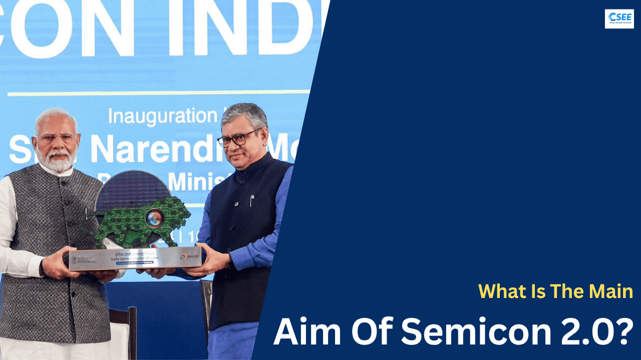
India has been building its semiconductor ecosystem through the Semicon India Programme. The first phase, often referred to as Semicon 1.0, focused on establishing the foundation for semiconductor and display manufacturing in the country. In July 2026, the Union Cabinet approved Semicon 2.0 with a total outlay of Rs 1,27,500 crore. The second phase is intended to deepen the capabilities created during the first phase and expand the ecosystem across the semiconductor value chain.
The main aim of Semicon 2.0 is therefore broader than simply building semiconductor factories. It is designed around six pillars covering design, machines and materials, fabs, advanced packaging, research and development, and talent development. Together, these pillars are intended to create a more complete semiconductor ecosystem in India, from designing semiconductor intellectual property and chips to manufacturing, packaging, research and developing the workforce required to support the industry.
Why does India need a complete semiconductor ecosystem?
A semiconductor industry is much larger than a chip fabrication plant. A modern semiconductor supply chain involves designers, intellectual-property developers, electronic-design-automation tools, equipment manufacturers, chemical and material suppliers, wafer fabrication facilities, assembly and testing companies, advanced packaging companies, research institutions and highly skilled engineers and technicians.
If a country develops only one part of this chain, it remains dependent on capabilities elsewhere. For example, a country may have strong chip-design engineers but still depend heavily on imported manufacturing equipment and materials. Similarly, having a fabrication facility is not enough if there are insufficient packaging, testing, equipment-maintenance or skilled workforce capabilities around it.
Semicon 2.0 is intended to address this broader ecosystem. Government information describes the programme as a long-term effort to build capabilities across the semiconductor value chain rather than focusing only on its later stages. The broader objective includes strengthening supply-chain resilience, increasing domestic value addition and creating high-value employment.
Pillar 1: Semiconductor Design
The first pillar is semiconductor design. This is one of the areas where India already has significant engineering capability because many global semiconductor companies operate large design and engineering centres in the country.
Chip design is the stage where engineers define what a semiconductor should do and how its internal circuits should operate. This can involve designing semiconductor IP, processors, controllers, memory-related blocks, communication blocks, power-management circuits, sensors, system-on-chip devices and complete modules.
Semicon 2.0 aims to expand India’s design ecosystem beyond individual chip designs. The government has identified support for semiconductor IP, chips, system-on-chip products and modules for both strategic and commercial applications. It also includes deployment-linked incentives for semiconductor IP, chips and SoCs.
Under the expanded approach, the government has set a target of supporting 200 semiconductor design startups. During the first phase, 105 semiconductor startups were supported, and the government has highlighted the fact that some of these startups have already attracted venture-capital funding.
This pillar is important because successful semiconductor companies need more than engineers who can design individual blocks. They need expertise across architecture, RTL design, verification, physical design, analog design, mixed-signal design, embedded systems, firmware, validation and product development.
The ecosystem can also create opportunities for engineers working with technologies such as Verilog, SystemVerilog, VLSI, FPGA, ASIC, SoC architecture, physical design, verification and semiconductor EDA tools.
Another important direction is moving from chip design towards systems design. As electronic products become more complex, semiconductor companies increasingly need to understand how multiple chips, software, sensors, processors and communication interfaces work together as a complete system. Semicon 2.0 therefore places emphasis on expanding India’s capabilities from individual designs towards more complex systems.
Pillar 2: Machines and Materials
The second pillar focuses on machines and materials required for semiconductor manufacturing.
A semiconductor fab cannot operate with silicon wafers alone. Manufacturing requires highly specialised equipment, chemicals, gases, materials, precision systems, maintenance capabilities and manufacturing processes.
Semiconductor manufacturing equipment can involve processes such as deposition, lithography, etching, cleaning, inspection, metrology and wafer handling. Each process requires highly precise equipment operating in tightly controlled manufacturing environments.
Materials are equally important. Semiconductor manufacturing depends on specialised chemicals, gases, wafers and other materials that must meet extremely strict quality requirements.
Semicon 2.0 aims to encourage companies involved in manufacturing and research and development of semiconductor machines and materials. This is also connected with the development of India’s precision-manufacturing ecosystem.
This pillar can create opportunities beyond traditional semiconductor engineering roles. Mechanical engineers, electrical engineers, electronics engineers, chemical engineers, materials scientists, automation engineers, controls engineers, process engineers and equipment-maintenance specialists can all have roles within this ecosystem.
The government has also highlighted interest from global capital-equipment companies in establishing operations in India. India’s existing engineering and design capabilities could support such companies in establishing design and manufacturing activities.
Building this ecosystem domestically can also reduce dependence on external sources for critical manufacturing inputs. However, semiconductor supply chains are global and complex, so the objective is not necessarily complete isolation from international suppliers. Instead, the broader goal is to develop stronger domestic capabilities and more resilient supply chains.
Pillar 3: Setting Up More Fabs
The third pillar focuses on establishing more semiconductor fabrication facilities, commonly called fabs.
A semiconductor fab is a highly specialised manufacturing facility where semiconductor wafers are processed through multiple stages to create integrated circuits. These facilities require enormous investments, advanced equipment, controlled environments and highly skilled personnel.
The Semicon 2.0 framework includes support for silicon semiconductor wafer fabs, compound semiconductor and photonics facilities, sensors including MEMS, discrete semiconductor fabs and display fabs.
Different types of semiconductor technologies serve different applications. Silicon-based chips are widely used in processors, controllers and many other electronic products. Compound semiconductors such as silicon carbide and gallium nitride can be important for power electronics and other specialised applications. Sensors and MEMS technologies are relevant to automotive, industrial, consumer and other applications.
The development of fabs also creates demand for a large ecosystem around them. A fab requires process engineers, equipment engineers, automation engineers, facilities engineers, quality engineers, manufacturing engineers, yield engineers and technicians.
There are also opportunities for suppliers of chemicals, gases, equipment, cleanroom systems, utilities, testing equipment and maintenance services.
This is why the third pillar cannot be viewed independently. A new fab creates demand across many other parts of the semiconductor ecosystem, connecting directly with the machines-and-materials pillar and the talent pillar.
Pillar 4: Advanced Packaging and ATMP/OSAT
The fourth pillar focuses on further strengthening India’s ATMP and OSAT industry.
ATMP stands for Assembly, Testing, Marking and Packaging, while OSAT stands for Outsourced Semiconductor Assembly and Test.
After a semiconductor wafer has been fabricated, the individual dies still need to be assembled, connected, protected and tested before they can be used as finished semiconductor components.
Packaging is becoming increasingly important as chip architectures become more advanced. Traditional packaging methods are being supplemented by technologies that allow multiple dies or chiplets to be integrated into sophisticated packages.
Advanced packaging can include technologies such as 2.5D and 3D integration, chiplet-based architectures, high-density interconnects and other techniques designed to improve system performance, power efficiency and integration.
Semicon 2.0 specifically aims to strengthen the ATMP/OSAT industry and encourage advanced ATMP technologies in India.
This is a significant area because semiconductor innovation is no longer limited to making smaller transistors. How different dies are connected and packaged can also influence performance, power consumption, bandwidth and system-level integration.
India’s packaging ecosystem is therefore expected to complement fabrication capabilities. Government information has highlighted the development of multiple packaging facilities under the broader semiconductor programme, with commercial production already beginning at some approved units.
For engineers, advanced packaging opens opportunities in semiconductor packaging design, thermal management, signal integrity, reliability engineering, testing, manufacturing automation and materials engineering.
Pillar 5: Research and Development
The fifth pillar is research and development.
Semiconductor technology changes continuously. New transistor structures, materials, packaging approaches, memory technologies, computing architectures, manufacturing processes and specialised chips require continuous research.
Semicon 2.0 aims to strengthen applied semiconductor R&D by encouraging collaboration between industry, government and academic institutions.
The government has said that industry can propose R&D projects with participation from industry, government and academic institutions. The objective is to develop applied technologies and achieve tangible outcomes that can strengthen India’s semiconductor capabilities.
This approach is important because research becomes more valuable to the industry when it can move from laboratories into real products, manufacturing processes and commercial technologies.
Areas of semiconductor R&D can include advanced process technologies, semiconductor materials, device physics, chip architecture, AI accelerators, power electronics, sensors, photonics, advanced packaging, manufacturing equipment and semiconductor testing.
Universities can play an important role in this pillar because semiconductor research requires long-term investment in laboratories, equipment, researchers and specialised academic programmes.
Industry participation can help ensure that research addresses practical manufacturing and product requirements. This combination can create a stronger connection between academic research and commercial semiconductor development.
Pillar 6: Talent Development
The sixth pillar is talent development.
A semiconductor ecosystem cannot grow without engineers, technicians, researchers and manufacturing professionals who understand the technology and processes involved.
Semiconductor companies require talent across many areas, including chip design, verification, physical design, embedded systems, process engineering, equipment engineering, packaging, testing, cleanroom operations, manufacturing, materials, quality and reliability.
India already has a large engineering workforce, but semiconductor manufacturing requires specialised skills that are different from many conventional software and electronics roles.
Under the first phase, semiconductor chip-design education was expanded across universities and institutes. The government has stated that hundreds of universities and institutes are already involved in semiconductor education and that Semicon 2.0 will further upgrade curricula and training.
The talent-development pillar also goes beyond chip designers. The government has set a target of training 1 lakh technicians over five years, including through partnerships with industry and international institutions.
This is particularly important because semiconductor fabs and packaging facilities need technicians who can work with cleanroom environments, manufacturing equipment, process controls, testing systems and specialised production tools.
The government has also stated that the earlier target of developing 85,000 semiconductor engineers over ten years was achieved in four years and that a new target of developing another 1 lakh engineers has been announced.
The difference between engineers and technicians is important here. A semiconductor ecosystem needs both. Engineers may work on design, process development, equipment, manufacturing and R&D, while technicians are essential for operating, maintaining and supporting highly specialised manufacturing facilities.
How the six pillars connect with each other
The real significance of Semicon 2.0 is that the six pillars are interconnected.
A chip-design company needs semiconductor IP, EDA tools, verification capabilities and skilled engineers. Once a chip is designed, it needs to be fabricated. The fab requires equipment, chemicals, gases and materials. After fabrication, the semiconductor needs assembly, testing and packaging. Advanced packaging may require additional R&D and specialised equipment. All these activities require trained engineers and technicians.
Research supports improvements across every stage. New materials can improve manufacturing. New packaging techniques can improve system performance. New chip architectures can enable AI and automotive applications. New manufacturing equipment can improve productivity and precision.
Talent supports all six pillars because every stage depends on people with specialised knowledge.
This interconnected structure is why Semicon 2.0 is broader than simply attracting semiconductor fabs. The stated objective is to build capabilities across the semiconductor value chain.
What could Semicon 2.0 mean for Indian engineers?
The expansion of the semiconductor ecosystem can create opportunities across multiple engineering disciplines.
For electronics and electrical engineers, opportunities can emerge in chip design, embedded systems, semiconductor testing, power electronics, manufacturing equipment and validation.
For computer engineers, opportunities can exist in processor architecture, verification, EDA software, firmware, semiconductor software and AI accelerator development.
For mechanical engineers, semiconductor equipment, precision manufacturing, automation, thermal systems and facilities engineering can become relevant areas.
Chemical and materials engineers can contribute to semiconductor chemicals, wafer processing, materials development and manufacturing processes.
Control and automation engineers can work on semiconductor manufacturing equipment, process automation, robotics and factory systems.
The ecosystem also creates opportunities for software engineers because semiconductor companies increasingly depend on software for EDA tools, automation, data analysis, factory systems, simulation and AI-based manufacturing optimisation.
This means the semiconductor industry should not be viewed as an industry limited to VLSI engineers. It requires a wide range of engineering and technical disciplines.
Why advanced packaging is becoming more important
One of the most interesting aspects of Semicon 2.0 is the stronger focus on advanced packaging.
For many years, semiconductor progress was strongly associated with reducing transistor size. However, modern computing systems increasingly use multiple processing elements, memory components and specialised accelerators.
Instead of putting every function onto one large chip, designers can use multiple dies or chiplets and connect them inside a package.
This approach can provide flexibility in system design and can help address some of the challenges associated with increasingly complex chips.
Advanced packaging also becomes particularly relevant for AI and high-performance computing, where processors need to communicate with memory and other processing elements at very high speeds.
For India, developing advanced packaging capabilities can therefore create a pathway into sophisticated semiconductor technologies while complementing domestic fabrication capabilities.
Semicon 2.0 and India’s manufacturing ecosystem
Semiconductor manufacturing can also have a wider economic impact because fabs and packaging facilities require many supporting industries.
A semiconductor facility needs reliable electricity, water, gases, chemicals, cleanroom infrastructure, logistics, equipment maintenance, waste management, testing systems and specialised construction.
This can lead to opportunities for companies outside the traditional semiconductor sector.
For example, precision engineering companies can potentially supply components for manufacturing equipment. Industrial automation companies can provide factory-control systems. Chemical companies can develop semiconductor-grade materials. Engineering companies can provide cleanroom and facility solutions.
This creates a multiplier effect where semiconductor investments can generate activity across several connected industries.
Semicon 1.0 versus Semicon 2.0
Semicon 1.0 and Semicon 2.0 should be viewed as connected phases rather than completely separate programmes.
Semicon 1.0 had an outlay of Rs 76,000 crore and focused on establishing the foundation for semiconductor and display manufacturing. It supported areas including fabs, display fabs, compound semiconductors, silicon photonics, sensors, ATMP/OSAT facilities and semiconductor design.
Semicon 2.0 has a larger outlay of Rs 1,27,500 crore and aims to deepen and broaden these capabilities. The government describes the second phase as an effort to put the wider ecosystem in place and scale capabilities across the semiconductor value chain.
The difference is therefore not simply about spending more money. It is about expanding the ecosystem around semiconductor manufacturing.
Design, equipment, materials, fabs, packaging, R&D and talent need to grow together for the industry to become more comprehensive.
The role of startups
Startups can play an important role in the semiconductor ecosystem because many emerging semiconductor technologies require specialised products and intellectual property.
A startup may focus on a particular chip architecture, sensor, communication technology, power-management device, AI accelerator, security technology or semiconductor IP.
However, semiconductor startups face challenges that are different from many software startups. Chip development requires expensive design tools, verification, prototyping, fabrication, packaging and testing.
Government support can therefore help reduce some of the barriers involved in moving from an idea to a working semiconductor product.
The Semicon 2.0 design pillar specifically aims to expand India’s semiconductor design startup ecosystem, with a target of 200 semiconductor design startups.
The importance of global partnerships
Building a semiconductor ecosystem does not mean operating independently from the rest of the world.
Semiconductor manufacturing is a global industry involving companies, technologies, equipment suppliers, research organisations and supply chains across many countries.
India therefore needs international partnerships alongside domestic capability development.
Government information highlights semiconductor cooperation with countries and regions including the United States, Japan, the European Union, Singapore and the Netherlands. India has also pursued partnerships related to semiconductor ecosystems and supply chains.
International collaboration can provide access to technology, expertise, investment, manufacturing experience and global markets.
At the same time, strengthening domestic capabilities can give Indian companies and institutions a stronger position within these international partnerships.
What does this mean for India’s semiconductor future?
Semicon 2.0 represents an attempt to move from building individual semiconductor facilities towards building an interconnected ecosystem.
The six pillars address different parts of that ecosystem. Design creates intellectual property and chips. Machines and materials provide the manufacturing foundation. Fabs manufacture semiconductor devices. Advanced packaging connects and prepares chips for real-world applications. R&D develops new technologies. Talent provides the people required to operate and improve the entire system.
The success of such an ecosystem will depend on execution, technology development, investment, infrastructure, industry participation, research quality and the availability of skilled talent.
The semiconductor industry also has long development cycles. Building fabs, qualifying manufacturing processes, developing suppliers and training specialised professionals takes time. Therefore, the impact of Semicon 2.0 will need to be evaluated over several years rather than through short-term announcements alone.
Conclusion
The main aim of Semicon 2.0 is to build a more complete and capable semiconductor ecosystem in India.
Instead of looking at semiconductors only as a chip-manufacturing opportunity, the six-pillar approach covers the wider chain: design, machines and materials, fabs, advanced packaging, research and development, and talent development.
The programme was approved with an outlay of Rs 1,27,500 crore, and the government has described it as a long-term effort to deepen India’s semiconductor capabilities.
For engineers and technology professionals, this ecosystem can create opportunities across VLSI, chip design, embedded systems, semiconductor manufacturing, equipment, automation, materials, packaging, testing, R&D and technical operations.
For startups, it can create opportunities to develop semiconductor IP, chips, systems and specialised technologies.
For universities, it can create stronger links between semiconductor education, research and industry.
And for the broader electronics industry, a stronger semiconductor ecosystem can provide more domestic capabilities across the value chain.
Ultimately, Semicon 2.0 is not just about producing more chips. Its broader purpose is to develop the capabilities, infrastructure, companies, technologies and people needed to participate across the semiconductor value chain. That is what makes the six pillars central to India’s next phase of semiconductor development.
Also, read:
- What Is The Main Aim Of Semicon 2.0?
- 20 Advanced Coursera Courses for Embedded Engineers That Can Lead to High-Paying Careers
- E/E Architecture Is Changing: From Distributed ECUs to Zonal Architecture
- Embedded C vs C++: Which Should Embedded Engineers Learn?
- TSMC’s AI-Chip Demand Is Still Exploding: What It Means for AI Hardware and Embedded Engineers
- IndiaAI Crosses 45,000 GPUs: What It Means for India’s AI and Edge AI Future
- 30-Day DSA in C for Embedded Systems Engineers
- 100 GitHub Projects to Level Up Your Embedded Engineering Skills