Five chips that could decide the next decade of AI
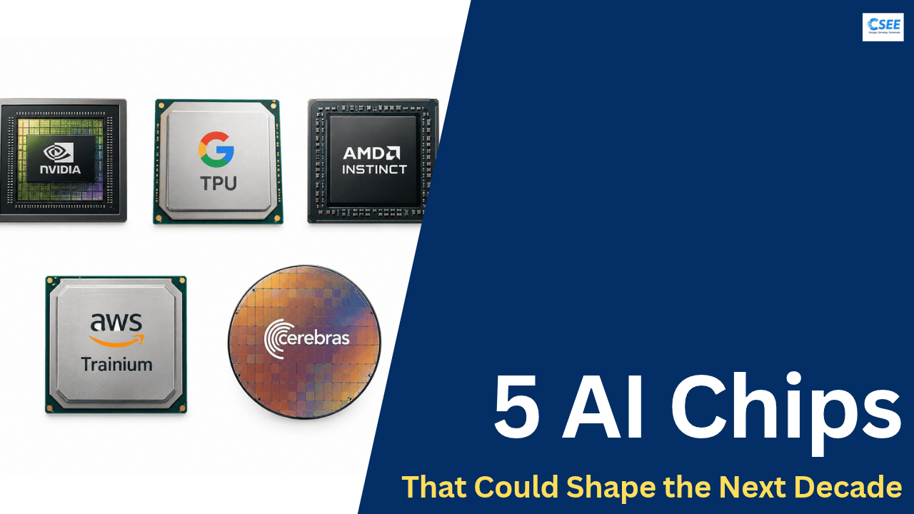
Smarter algorithms get the headlines, but every model runs on silicon. Here is how NVIDIA, Google, AMD, AWS and Cerebras are each betting on a different answer to the same problem: more compute, less energy, lower cost.
Why the chip matters as much as the model
A large language model is, at bottom, an enormous pile of matrix multiplications. Training one means running those multiplications trillions of times over a mountain of text. Serving one to millions of people means running them again for every word it writes back. The speed, power draw and price of that arithmetic now shape what AI companies can afford to build.
That is why the AI chip race has stopped being a story about one company. The five platforms in this article take different routes, but each is trying to push on the same three levers.
all three combine into
cost per useful token
One more idea helps before we meet the chips. AI work splits into two very different jobs. Training builds the model once and is limited by raw compute and how fast thousands of chips can talk to each other. Inference runs the finished model over and over, and is usually limited by memory: how quickly the chip can pull the model’s weights out of memory for each new word.
Training · build the model
Inference · use the model
Blackwell and Rubin: the incumbent keeps raising the bar
NVIDIA’s GPUs train and serve most of the world’s frontier models today, and its strategy is simple: ship a much faster platform every year and make it easy to keep using the same software. The current generation, Blackwell, arrived in the B200 and the upgraded B300 (Blackwell Ultra). The B300 carries 288 GB of HBM3e memory and roughly 15 petaFLOPS of FP4 compute per GPU.
The successor, Vera Rubin, is the headline act for late 2026. The Rubin GPU is built on TSMC’s 3 nm process as a multi-chip package with 336 billion transistors. It is the first NVIDIA platform on HBM4 memory, with 288 GB per GPU and around 22 TB/s of memory bandwidth, close to triple Blackwell’s 8 TB/s. NVIDIA quotes about 50 petaFLOPS of NVFP4 inference per GPU, roughly five times a B200, and 35 petaFLOPS for training.
The bigger story is that NVIDIA no longer really sells a chip. It sells a rack that behaves like one giant GPU. Rubin pairs with NVIDIA’s own Vera CPU, which has 88 custom Arm cores and talks to the GPU over a 1.8 TB/s coherent link. NVLink 6 doubles GPU-to-GPU bandwidth to 3.6 TB/s, and inside a full NVL72 rack that adds up to a 260 TB/s fabric.
NVIDIA’s other advantage is CUDA, the software layer that nearly every AI framework is built around. Competitors can match a spec sheet; matching fifteen years of tuned libraries is harder. The risk for NVIDIA is price. Each Rubin GPU costs more than a Blackwell, so its customers are being pushed to judge it on cost per token, not cost per chip. Its roadmap already lists Rubin Ultra for 2027 and a next architecture, Feynman, after that.
TPUs: a decade of custom silicon, now split in two
Google started designing Tensor Processing Units in the mid-2010s because it saw that running AI across Search, YouTube and Translate on general-purpose chips would be too costly. A TPU is an ASIC: a chip that does one family of jobs, matrix math, and drops the graphics heritage of a GPU. That focus is where its efficiency comes from.
The seventh generation, Ironwood, is the chip Google pitched for the “age of inference.” Each Ironwood chip delivers about 4,614 teraFLOPS of FP8 compute with 192 GB of HBM3E memory, and Google says it offers more than four times the per-chip performance of the previous Trillium generation. Its real strength is scale. Ironwood chips link into pods of up to 9,216 chips over Google’s own inter-chip interconnect, giving a single pod about 42.5 exaFLOPS of FP8 compute and roughly 1.77 PB of shared high-bandwidth memory.
4.6 PF FP8 · 192 GB
smaller config
42.5 EF · 1.77 PB HBM
Customers have taken notice. Anthropic announced plans to use up to one million TPUs for its Claude models, a sign that Google’s chips are now a serious option for companies outside Google itself.
In April 2026 Google went a step further. For the first time in the program’s history, its eighth generation is two separate chips, both on TSMC’s 2 nm process: the TPU 8t for training and the TPU 8i for inference. Google’s reasoning is that AI agents, which think in many short steps, need a different balance of memory and latency than a training run does.
- 216 GB HBM, 128 MB on-chip SRAM
- Up to 9,600 chips per superpod
- ~2.7–2.8× better training price-performance vs Ironwood
- 288 GB HBM, 384 MB on-chip SRAM
- New “Boardfly” network topology for low latency
- ~80% better inference performance per dollar
The catch with TPUs is access. You cannot buy one for your own server room; you rent them on Google Cloud. For many companies that is fine, but it ties the hardware choice to a cloud choice.
Instinct: the open challenger with the biggest memory
AMD is the only company here that competes with NVIDIA on NVIDIA’s own terms: a general-purpose GPU that anyone can buy and install. Its pitch rests on two things, more memory per chip and open standards.
The new Instinct MI455X carries 432 GB of HBM4, half again as much as a Rubin GPU, and AMD rates it at up to 40 petaFLOPS of FP4. More memory per chip matters most for inference: a bigger model fits on fewer chips, so less time is spent shuffling data between them.
Like NVIDIA, AMD now sells whole racks. Its Helios system packs 72 MI455X GPUs with 18 sixth-generation EPYC “Venice” CPUs and Pensando networking. One rack holds about 31 TB of HBM4 and delivers around 2.9 exaFLOPS of FP4. Helios ties its GPUs together with UALink, an open alternative to NVIDIA’s NVLink, and uses Ultra Ethernet to connect racks.
The customer list shows the challenge is real. OpenAI, Meta, Anthropic, Microsoft and Oracle have all lined up for Helios, with volume shipments ramping through the second half of 2026. AMD’s weak spot is software. Its ROCm stack has improved quickly, but analysts still describe CUDA as a moat, and every customer that switches has to port and tune code. AMD has committed to a yearly cadence, with MI500 next.
Trainium: making the AI bill smaller
Amazon’s chip team, Annapurna Labs, is not trying to build the fastest chip in the world. It is trying to build the one that gives the most work per dollar on Amazon’s cloud. Because AWS designs the chip, the server, the network and the data centre together, it can strip out costs that a chip bought from someone else would carry.
Trainium3, launched at re:Invent in December 2025, is built on a 3 nm process and delivers 2.52 petaFLOPS of FP8 with 144 GB of HBM3e per chip. That is lower than the GPUs above, but AWS packs 144 of them into a single Trn3 UltraServer and lets customers join thousands of UltraServers together. AWS says the new systems give about 4.4 times the compute of the previous generation while using around 40% less power, and claims up to 50% lower cost for training and inference.
Big users are already on board. Anthropic trains and serves Claude models on Trainium, and Amazon Bedrock runs production traffic on Trainium3. The next step, Trainium4, is a surprise: AWS is designing it to support NVIDIA’s NVLink Fusion interconnect, so Trainium chips can sit in the same racks as NVIDIA GPUs. AWS is targeting at least six times the FP4 performance, three times the FP8 performance and four times the memory bandwidth of Trainium3.
Trainium shows that competing with NVIDIA does not always mean beating it on speed. Sometimes it means being good enough at a much lower price, and working alongside it where needed.
Wafer-scale: the chip the size of a dinner plate
Every other chip in this article is cut from a silicon wafer, a disc 300 mm across that holds dozens of chips. Those chips are then wired back together with cables and switches so they can work as one. Cerebras asked a blunt question: why cut the wafer up at all?
Its Wafer-Scale Engine 3 is a single chip that covers most of the wafer, 46,225 mm². It holds 4 trillion transistors, 900,000 AI cores and 44 GB of SRAM placed right next to the cores, delivering 125 petaFLOPS. Because the model’s working data stays on the chip, memory bandwidth reaches about 21 PB/s, thousands of times more than a GPU reading from external HBM.
The result is exceptional speed on inference, especially the decode step where a model writes its answer one token at a time. Cerebras claims up to 15 to 21 times faster inference than GPU systems on popular open models. That speed has won big contracts: OpenAI signed a multi-year deal reported at up to $20 billion in January 2026, and AWS agreed to place WSE-3 systems in its data centres to handle decode while other chips handle prefill. Cerebras listed on Nasdaq in May 2026 under the ticker CBRS.
The trade-offs are real. 44 GB of SRAM is fast but small, so the largest models must be split across many CS-3 systems. Each system is a specialised, water-cooled appliance, and Cerebras is tiny next to NVIDIA in revenue. Its bet is that for instant, interactive AI, speed matters more than anything else.
The five platforms compared
Comparing these chips is tricky. Vendors quote different number formats (FP4 or FP8), different scales (a chip, a rack or a pod) and peak figures that real workloads rarely hit. The table lines up the headline numbers each company has published, so treat it as a map, not a race result.
| Platform | Type | Peak compute / chip | Memory / chip | Largest unit | Best at | How you get it |
|---|---|---|---|---|---|---|
| NVIDIA Rubin | GPU | 50 PF FP4 | 288 GB HBM4 | NVL72 rack, 72 GPUs | Everything, with the deepest software | Buy or rent anywhere |
| Google Ironwood | ASIC | 4.6 PF FP8 | 192 GB HBM3E | 9,216-chip pod | Huge-scale training and serving | Google Cloud only |
| AMD MI455X | GPU | 40 PF FP4 | 432 GB HBM4 | Helios rack, 72 GPUs | Memory-hungry inference | Buy or rent; open standards |
| AWS Trainium3 | ASIC | 2.52 PF FP8 | 144 GB HBM3e | UltraServer, 144 chips | Low cost per training run | AWS cloud only |
| Cerebras WSE-3 | Wafer-scale | 125 PF (system) | 44 GB on-chip SRAM | CS-3 clusters | Ultra-fast token generation | Cerebras cloud, partners, systems |
FP4 numbers are roughly double FP8 numbers on the same hardware, so do not compare the FP4 and FP8 rows directly. On phones this table becomes one card per chip.
Three philosophies of AI silicon
Step back from the specs and the five companies fall into three camps. Each makes a different trade between flexibility and efficiency.
| Approach | Who | The bet | Strength | Weakness |
|---|---|---|---|---|
| General GPU | NVIDIA, AMD | One flexible chip, sold to everyone, wired into giant racks | Runs any model; huge ecosystem | Carries features some AI jobs never use; premium price |
| Cloud ASIC | Google, AWS | Design chip, server and data centre together for your own cloud | Better cost and energy per token | Only available on one cloud; narrower software |
| Wafer-scale | Cerebras | Keep the whole wafer as one chip so data never leaves it | Unmatched inference speed | Limited on-chip memory; specialised systems |
The next milestones
The race is moving on a yearly clock now. These are the dates that will show which bets pay off.
Vera Rubin NVL72 and AMD Helios racks ramp to volume. Google’s TPU 8t and 8i begin reaching cloud customers. Watch real-world cost per token, not peak FLOPS.
AWS Trainium4 arrives with NVLink Fusion, testing whether mixed racks of custom chips and NVIDIA GPUs can work smoothly.
NVIDIA Rubin Ultra (about 1 TB of memory per package) and AMD MI500 continue the annual cadence. Cerebras must show a successor to WSE-3 and broaden its customer base.
NVIDIA’s Feynman generation and 2 nm-class chips across the industry. Power supply, not chip design, may become the main limit on how much AI gets built.
Why this matters beyond the data centre
It is tempting to treat chips as plumbing. But the price of an AI answer, how quickly it arrives and how much electricity it burns are all set at the silicon level. When Google says a new TPU cuts inference cost by 80% per dollar, or AWS says Trainium halves a training bill, that saving decides whether a startup can afford to train its own model, or whether a free AI tool stays free.
No single chip is likely to “win.” NVIDIA’s Rubin will stay the default for most buyers because it runs everything and its software is everywhere. Google and AWS will keep moving their own heavy workloads onto custom chips that are cheaper for them to run. AMD gives the industry a second source and a push toward open standards. Cerebras proves there is room for radically different designs when speed is what matters.
The next decade of AI will be shaped by whoever delivers the most useful intelligence per watt and per dollar. These five chips are the leading attempts to answer that question, and the competition between them is exactly what will keep pushing the answer forward.
- Vera Rubin GPU technical specifications
- NVIDIA GTC 2026 announcements (Bizon)
- NVIDIA Vera Rubin architecture explained (VRLA Tech)
- Google Ironwood TPU and 9,216-chip superpod (TrendForce)
- 3 things to know about Ironwood (Google)
- Google splits its TPU into two chips (Tom’s Hardware)
- Eighth-generation TPUs (DatacenterDynamics)
- AMD Instinct MI400 series and Helios (AMD)
- AMD MI455X with 432 GB HBM4 (Guru3D)
- AMD Epyc and Instinct roadmap (The Register)
- Amazon Trainium3 and Trainium4 roadmap (Introl)
- AWS Trainium3 launch (TechCrunch)
- Cerebras files to go public (SiliconANGLE)
- Cerebras vs NVIDIA: wafer-scale vs GPU