ASML: The Machine Behind the World’s Most Advanced Chips
One Dutch company builds the only machines on Earth that can print the finest patterns on today’s leading AI chips. Here is how the chain works, why the machines are so extraordinary, and why the industry depends on them.
1. The simple chain
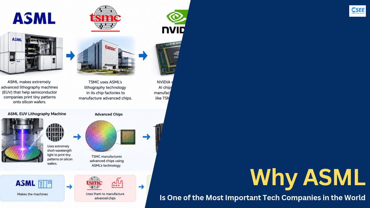
Most people know NVIDIA for its AI chips. Fewer know that NVIDIA is a designer, not a factory owner. It draws the blueprint; someone else has to turn that blueprint into physical silicon. That someone is mostly TSMC in Taiwan, and TSMC in turn cannot make leading-edge chips without ASML’s lithography machines.
2. What is lithography?
Lithography means “writing with light.” A chip is built from dozens of stacked layers, and each layer needs a pattern of microscopic lines, shapes and holes. To create one, a wafer (a thin disc of silicon) is coated with a light-sensitive chemical called photoresist. Light passes through or reflects off a mask (also called a reticle) that carries the pattern, and the machine shrinks that image onto the wafer. Where light hits the resist, its chemistry changes, and the pattern can then be etched or built up in the material below.
Think of it as an extremely precise projector. A slide projector enlarges an image; a lithography scanner does the opposite, shrinking a mask pattern to a fraction of its size and focusing it onto a wafer. That step repeats for every layer, and modern chips can need well over a hundred patterning steps, many of them using lithography.
3. Why wavelength matters
The smallest feature a lithography system can print is governed by a well-known relationship:
Shorter wavelength helps. A larger NA, meaning optics that gather light from a wider angle, helps too. k1 is a process factor engineers push as low as they can with tricks like multiple patterning and computational optimization. Here is how the generations compare, using an illustrative k1 of 0.3:
| Technology | Wavelength | NA | Approx. smallest feature |
|---|---|---|---|
| DUV dry (KrF) | 248 nm | ~0.8 | ~90 nm |
| DUV immersion (ArF) | 193 nm | up to 1.35 | ~43 nm single exposure |
| EUV | 13.5 nm | 0.33 | ~12 nm |
| High-NA EUV | 13.5 nm | 0.55 | ~7 nm |
These are idealized calculations, and real chips use manufacturers’ own node names, which are marketing labels rather than literal measurements. But the pattern is clear: moving from 193 nm to 13.5 nm light is a leap of roughly fourteen times in wavelength, and it let the industry print far finer detail with fewer steps.
4. What makes EUV so hard
Extreme ultraviolet light at 13.5 nm is absorbed by almost everything, including air and glass. That single fact forces a completely different machine design.
The light source
EUV light is made by firing a powerful carbon-dioxide laser at tiny droplets of molten tin, roughly 25 micrometers across, falling through a vacuum chamber. A first, gentler laser pulse flattens the droplet, then a main pulse vaporizes it into a plasma hot enough to emit 13.5 nm light. This happens about 50,000 times every second. Specialized collector optics gather the light and direct it into the system.
Mirrors instead of lenses
Glass lenses would absorb EUV light, so the machine uses mirrors. These are among the smoothest objects ever made, coated with alternating thin layers of molybdenum and silicon that reflect light by constructive interference. Even so, each mirror reflects only around two thirds of the light, so with a long chain of mirrors only a small fraction of the source’s power reaches the wafer. Zeiss, a German optics company, is ASML’s key partner here.
Everything in vacuum
Because air absorbs EUV light, the whole beam path is held in a vacuum. This makes cooling, wafer handling and contamination control much harder.
Atomic-scale precision
The wafer stage and mask stage move at high speed in sync, with positioning accuracy measured in nanometers. Layers must be aligned on top of each other (called overlay) to within a few nanometers across a whole wafer.
5. ASML’s product families
| Family | Light | Typical use | Notes |
|---|---|---|---|
| DUV dry | 248 / 193 nm | Less critical chip layers, mature chips | Mature, high volume |
| DUV immersion | 193 nm through water | Many layers in advanced chips | Water layer boosts NA |
| EUV (0.33 NA) | 13.5 nm | Critical layers on advanced logic and memory | Roughly $200M+ each |
| High-NA EUV (0.55 NA) | 13.5 nm | Next-generation nodes | Roughly $350M+ each, still being adopted |
| Metrology and inspection | Various | Measuring and checking patterns | Helps keep yield high |
EUV does not replace DUV. A single advanced chip typically uses both: EUV for the most delicate layers, and DUV for the many layers that do not need that fineness. This is why ASML’s overall business spans several technologies.
6. Why only one company?
ASML began in 1984 as a joint venture between Philips and ASM International, in Veldhoven, the Netherlands. Competitors in lithography, such as Nikon and Canon, once held major share, but EUV took roughly two decades to develop and required enormous investment and a global network of suppliers. In 2012, ASML’s biggest customers (Intel, TSMC and Samsung) invested in ASML to fund the work, an unusual arrangement that shows how badly the industry needed the technology.
- Complexity: light source, optics, vacuum, motion and software must all work together flawlessly.
- Supplier network: thousands of specialist suppliers, with unique roles such as Zeiss mirrors and high-power laser systems.
- Accumulated knowledge: decades of learning cannot be copied quickly.
- Customer co-development: chipmakers work closely with ASML on each generation.
7. TSMC and NVIDIA’s role
TSMC runs the world’s largest contract chip factories (foundries). It buys ASML tools by the dozen, installs them in huge cleanrooms, and builds its processes around them. NVIDIA is a fabless company: it designs GPUs and AI accelerators, then hands the finished designs to a foundry. Advanced AI chips also depend on packaging and high-bandwidth memory, which involve other suppliers, so lithography is a critical piece rather than the whole story.
| Company | Role | What it contributes | Depends on |
|---|---|---|---|
| ASML | Equipment maker | Lithography systems | Zeiss optics, lasers, thousands of suppliers |
| TSMC | Foundry | Manufacturing process and capacity | ASML and other tool makers |
| NVIDIA | Chip designer | GPU architecture and software | TSMC, memory makers, packaging |
| Cloud and AI firms | Customers | Demand for AI compute | NVIDIA systems |
8. From sand to AI chip: where lithography fits
9. Cost, risk and geopolitics
A single EUV tool can cost hundreds of millions of dollars, and a fab needs many. That expense is one reason only a few companies can afford leading-edge manufacturing. Because these tools are so strategic, governments pay close attention. The Netherlands, in coordination with allies, has restricted exports of the most advanced systems to certain countries, and rules continue to evolve, so it is worth checking current news for the latest position.
| Risk | Why it matters |
|---|---|
| Concentration | A single EUV supplier means any disruption ripples across the whole industry. |
| Cost growth | Each generation is more expensive, which can slow adoption. |
| Export rules | Policy changes can alter who can buy which machines. |
| Customer cycles | Chipmaker spending rises and falls with demand. |
10. Key takeaways
- ASML builds the machines; TSMC uses them to manufacture; NVIDIA designs the chips that result.
- Lithography prints chip patterns with light, and shorter wavelengths make finer detail possible.
- EUV at 13.5 nm needs tin plasma, mirrors and vacuum, and is among the most complex machines ever built.
- High-NA EUV extends the roadmap further, at higher cost.
- The AI boom rests on a long chain, and this is one of its most important links.
Figures such as prices, weights and part counts are approximate and change by model and year. This article is educational and not investment advice.