Why Did It Take Decades to Print Tiny Patterns on a Chip?
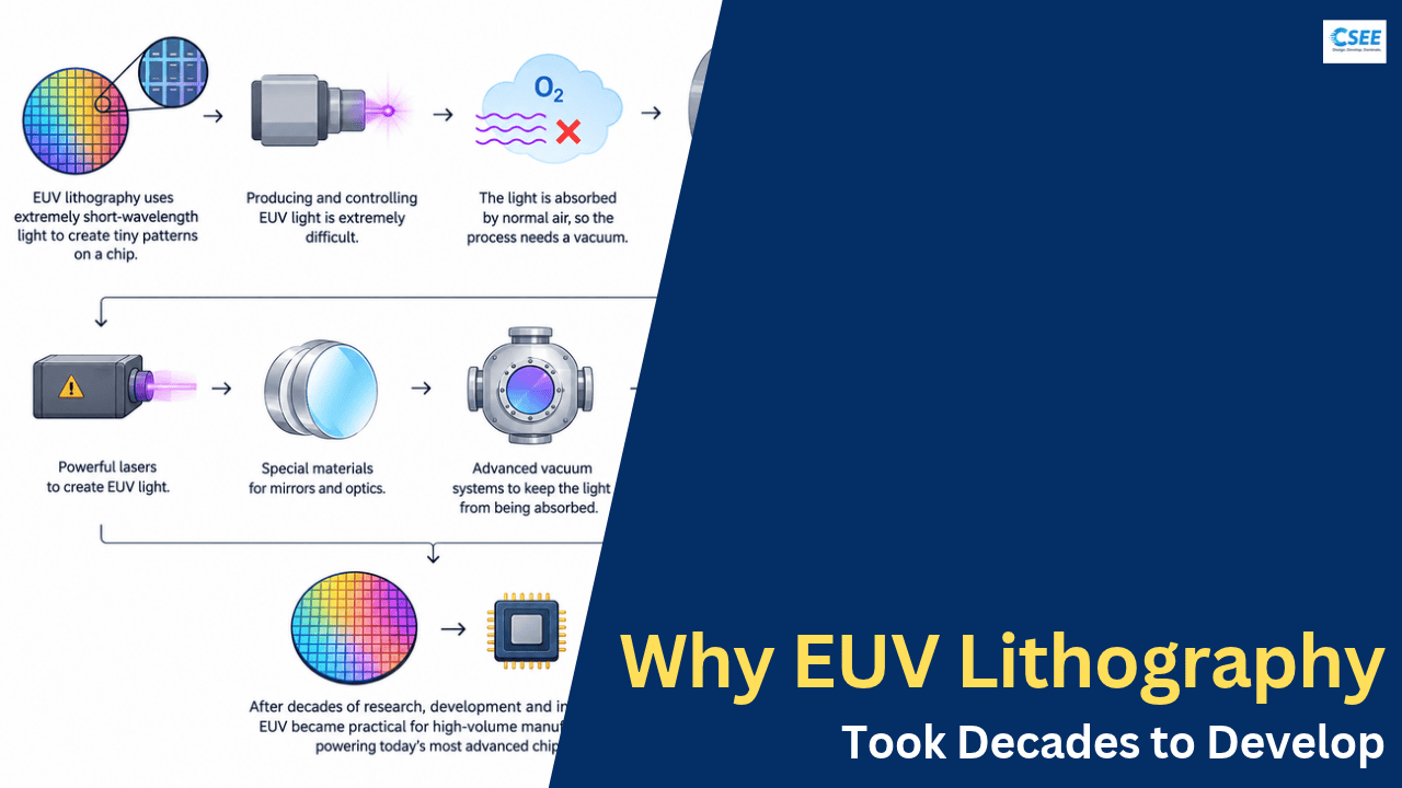
The answer is EUV lithography: Extreme Ultraviolet light at a wavelength of 13.5 nanometers. Printing with it required new lasers, new materials, mirrors polished to atomic precision, vacuum chambers and software that ties it all together. This guide walks through each piece.
1. The job: drawing with light
A modern chip is built in layers. For each critical layer, the factory coats a silicon wafer with a light-sensitive material called photoresist, shines a pattern of light through or off a template called a mask (or reticle), and then chemically develops the wafer so that only the exposed or unexposed areas remain. Etching and deposition steps then transfer that pattern into the chip. A leading-edge chip repeats this dozens of times with each layer lined up on the one below to within a few nanometers.
This is photolithography, literally “writing with light on stone.” It is the step that sets how small transistors and wires can be, which in turn decides how many fit on a chip. More transistors per chip means faster processors and the huge AI accelerators of today.
2. The physics: why wavelength limits detail
Light is a wave, and waves spread out when they squeeze through small openings (diffraction). That blur sets a floor on the smallest feature you can print. Engineers summarize it with the Rayleigh-style relation:
λ is the wavelength of light, NA is the numerical aperture (how wide a cone of light the lens or mirror system gathers), and k1 is a process factor that skilled engineering pushes down toward roughly 0.25–0.4.
There are three levers: shorten λ, raise NA, or reduce k1. For years the industry pulled all three. It moved from visible and near-UV light down to 193 nm deep ultraviolet (DUV) from an argon fluoride laser, put water between lens and wafer to lift NA above 1 (immersion lithography), and used clever tricks such as multiple patterning and computational mask correction to lower k1.
Those tricks work, but they cost money. Printing one layer with 3 or 4 separate exposures multiplies time, cost and the chance of misalignment. The cleaner solution is a much shorter wavelength, and that is what EUV offers.
| Light source | Wavelength | Typical era | Notes |
|---|---|---|---|
| g-line (mercury lamp) | 436 nm | 1980s | Micron-scale features |
| i-line (mercury lamp) | 365 nm | Late 1980s–1990s | Sub-micron |
| KrF excimer laser | 248 nm | 1990s | Deep UV begins |
| ArF excimer laser | 193 nm | 2000s onward | Immersion added water, NA ~1.35 |
| EUV (laser-produced plasma) | 13.5 nm | Volume use from about 2019 | Vacuum, mirrors only |
3. Problem one: air and glass block EUV
At 13.5 nm, light is on the border of X-rays. Almost every material absorbs it, including air, water, and the glass that makes ordinary lenses. Three consequences follow.
- Everything runs in vacuum. The beam path, the mask and the wafer sit in chambers pumped down to very low pressure, usually with a trace of flowing hydrogen gas that helps keep surfaces clean.
- No lenses. The optics must be mirrors only, and even the mask is a mirror rather than a transparent plate.
- Light is precious. Each reflection loses energy, so the system is designed to waste as little as possible.
Working in vacuum sounds simple but isn’t. Wafers must move at high speed and stop within nanometers, wafer stages accelerate harder than a fighter jet, and the vacuum must stay clean enough that no stray molecule dirties a mirror.
4. Problem two: making EUV light
No convenient laser or lamp makes strong 13.5 nm light. The industry found that very hot plasma of tin ions emits it efficiently. Making that plasma, reliably, tens of thousands of times a second, is one of the hardest engineering feats in manufacturing.
The droplet-and-laser recipe
- A generator releases tiny molten tin droplets, about 25 micrometers across, falling at high speed (roughly 50,000 per second).
- A first laser pulse (a “pre-pulse”) flattens each droplet into a thin pancake, a better target.
- A powerful carbon-dioxide laser, tens of kilowatts class, hits the pancake with the main pulse.
- The tin becomes a plasma at around a few hundred thousand degrees, brighter in EUV than anything else practical.
- A large curved collector mirror gathers the light and sends it into the scanner.
The timing and aim must be accurate to fractions of the droplet’s width, and the system must do it continuously for weeks.
5. Problem three: mirrors at atomic accuracy
A single surface cannot reflect much 13.5 nm light. The trick is a multilayer mirror: dozens of ultra-thin alternating layers of molybdenum and silicon, each only a few nanometers thick. Reflections from every interface add up in phase, a little like stacked thin films on a soap bubble.
Even at about two-thirds reflectivity per mirror, losses stack up. With roughly a dozen reflections from source to wafer (collector, illuminator, mask, and projection optics), only a small percentage of the source light reaches the wafer. That is why the source must be so powerful.
How smooth is smooth?
Mirror surface errors must be below a fraction of a nanometer. A common analogy: if a mirror were scaled to the size of a country, its largest bump would be thinner than a coin. Special manufacturers polish, measure and re-polish using ion beams, and the shape is verified with interferometers made just for this job. Heat from absorbed light also deforms mirrors, so cooling and active adjustment are required.
| Challenge | Why it is hard | Solution |
|---|---|---|
| Absorption in air | Gas and glass absorb 13.5 nm | Vacuum, reflective optics |
| Light source | No simple EUV laser | Tin plasma from CO2 laser |
| Low throughput | Each mirror loses ~30% | Multilayers, high-power source |
| Surface precision | Sub-nanometer errors print defects | Ion-beam polishing, metrology |
| Contamination | Tin and carbon dirty mirrors | Hydrogen flow, cleaning, shields |
| Masks | Reflective, defects hard to see | Multilayer blanks, inspection, pellicles |
| Resist noise | Few photons per feature | New resists, dose control |
6. Problem four: the mask and its defects
An EUV mask is itself a multilayer mirror, with an absorbing pattern on top. Light strikes it at a slight angle (around 6 degrees), bounces off and carries the pattern. A tiny bump buried under the multilayer can print as a defect, and it may be invisible from the surface. Mask makers needed new blank manufacturing, inspection tools and repair methods. A thin protective membrane (pellicle) keeps particles from landing on the pattern, but it must be nearly transparent to EUV and survive heat, which took years to develop.
7. Problem five: photons are rare and random
Each EUV photon carries about 14 times the energy of a 193 nm photon. For the same exposure energy there are far fewer photons. On a tiny feature just a few dozen photons may land, and random variation in that count creates rough edges or missing contacts. This is called stochastic variation or shot noise.
The fix is a combination of brighter sources (more photons per second), better resists that absorb EUV efficiently and respond sharply, and careful process control. It remains an active research area at the smallest dimensions.
8. Problem six: software and control
Hardware alone cannot print a chip. Computational lithography predicts how light will bend and blur, then reshapes the mask so the wafer pattern comes out right. Sensors measure mirror temperature, wafer position and dose thousands of times a second. Feedback loops adjust mirror shape on the fly, sync laser pulses to droplets, and align each new layer to earlier ones within a couple of nanometers. Without this software layer the tool would not meet its accuracy targets.
9. The decades-long timeline
| Period | Milestone |
|---|---|
| Mid-1980s | Researchers in Japan and the US demonstrate soft X-ray projection imaging with multilayer mirrors |
| 1990s | Industry and national labs form research consortia to explore EUV; many expect it near 2000s |
| 2000s | Source power, mask defects and resist stay stubborn; 193 nm immersion extends the old technology |
| 2010–2016 | Pre-production tools ship; source power rises step by step |
| 2018–2019 | First high-volume chips use EUV on a few layers |
| 2020s | EUV spreads to more layers; High-NA (0.55) tools begin delivery |
10. High-NA: the next step
Standard EUV tools use an NA of 0.33. The next generation raises it to 0.55, which allows finer features in a single exposure. Bigger mirrors alone would cause problems, so these tools use anamorphic optics that reduce the pattern by 4x in one direction and 8x in the other, and the exposed field is half as big. Cost and complexity rise again, and chipmakers weigh when each layer justifies it.
| Feature | Standard EUV | High-NA EUV |
|---|---|---|
| Numerical aperture | 0.33 | 0.55 |
| Wavelength | 13.5 nm | 13.5 nm |
| Reduction | 4x both directions | 4x / 8x anamorphic |
| Typical resolution | ~13 nm | ~8 nm |
| Field size | Full | Half |
11. Why it matters for AI and everyday chips
Advanced processors, mobile chips and AI accelerators rely on dense transistors for performance per watt. EUV lets makers print the tightest layers with fewer steps, so yields and cycle times improve. A single machine is the size of a bus, costs well over a hundred million dollars, and ships in many crates. The supply chain behind it crosses lasers, optics, vacuum, motion control and chemistry across many countries, which is also why only one company sells these tools.
12. Summary
- Shorter wavelength means finer detail, so industry moved to 13.5 nm.
- That light is absorbed by air and glass, forcing vacuum and all-mirror optics.
- Tin plasma, hit by a CO2 laser tens of thousands of times a second, makes the light.
- Multilayer mirrors with atomic smoothness steer it, losing about a third at each bounce.
- Reflective masks, pellicles, new resists and heavy software complete the system.
- Decades of cooperative work turned a lab curiosity into mass production.
An EUV machine is not simply a stronger lithography tool. It is physics, engineering, materials science and manufacturing discipline compressed into one system.