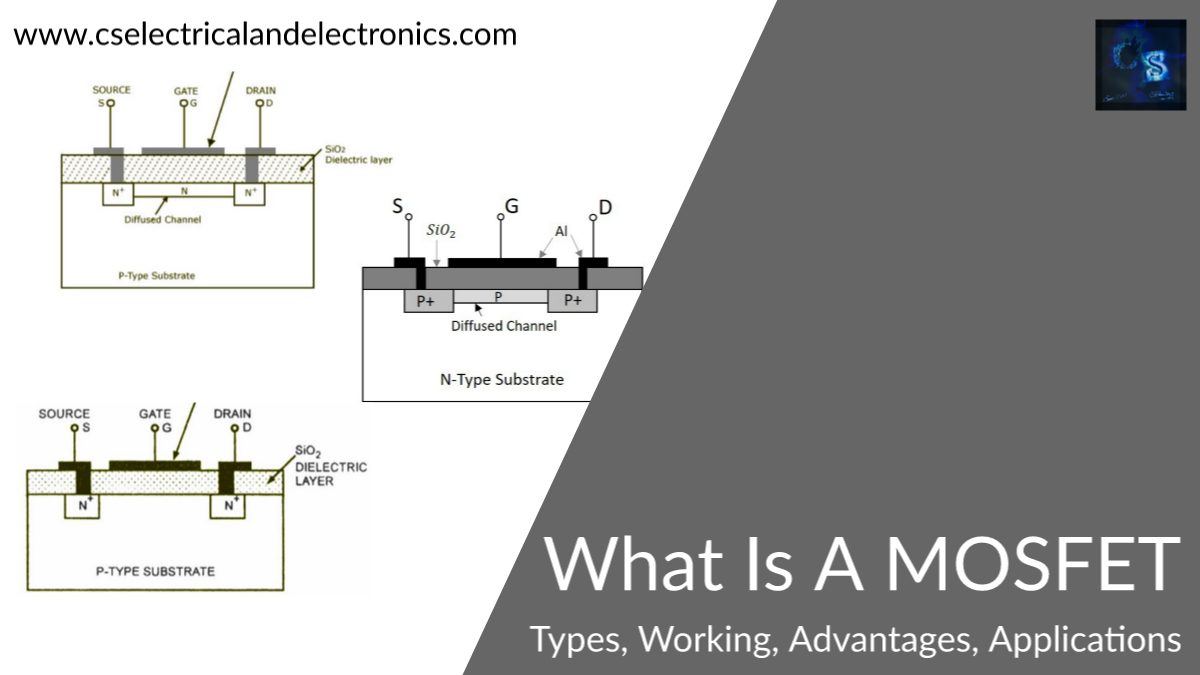
Hello guys, welcome back to my blog. In this article, I will discuss what is a MOSFET, the types of MOSFET, the working of it, the applications, the advantages, and disadvantages.
If you have any doubts related to electrical, electronics, and computer science, then ask questions. You can also catch me on Instagram – CS Electrical & Electronics And Chetan Shidling.
Also, read:
- What Is Clipper Circuit, Types, Advantages, Disadvantages, Applications
- What Is Interrupt, Interrupts Handling, Interrupt Service Routine
- Embedded System Questions Asked In Online Test At LTTS, Robert Bosch
What Is A MOSFET
MOSFET (Metal oxide semiconductor field-effect transistor) is a semiconductor device that is used as a switch or as an amplifier. These are very small and can be used in designing high-density VLSI designs.
Mosfet mainly consists of 3 terminals
- Drain
- Gate
- Source.
The input resistance of the MOSFET will be very high. It will not be having a P-N junction. Instead, it will be having an insulated gate terminal. Because of this MOSFET can be also called IGFETs.
Types Of MOSFET
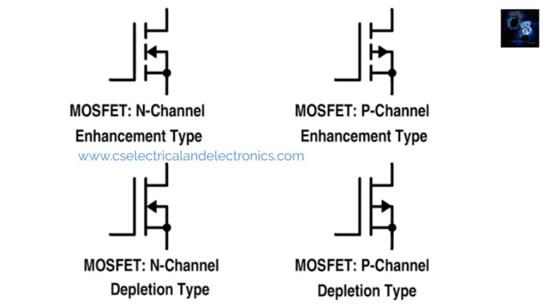
- Depletion type MOSFET (D-MOSFET)
• N-channel D-MOSFET.
• P-channel D-MOSFET. - Enhancement type MOSFET.(E-MOSFET)
• N-channel E-MOSFET
• P-channel E-MOSFET
Depletion Type MOSFET
- The depletion type MOSFET transistor will be equivalent to a “normally closed” switch.
- This requires the gate to source voltage to switch off the device. The n-channel depletion MOSFET and p-channel depletion MOSFET symbols are shown above.
- In the above symbols, we can see that the 4th terminal is connected to the ground. While in discrete MOSFET, it is connected to the source terminal.
- The continuous thick line, which is connected in between drain and source, represents the depletion type as shown in the below image. The arrow indicates the channel type, such as n-channel or p-channel.
- In the depletion type of MOSFET, a thin layer of silicon is deposited below the gate terminal. The p channel depletion-mode MOSFET will be on when gate-source voltage is 0. In this type of MOSFET, the conductivity will be less, compared to the enhancement type of MOSFET.
N-channel D-MOSFET
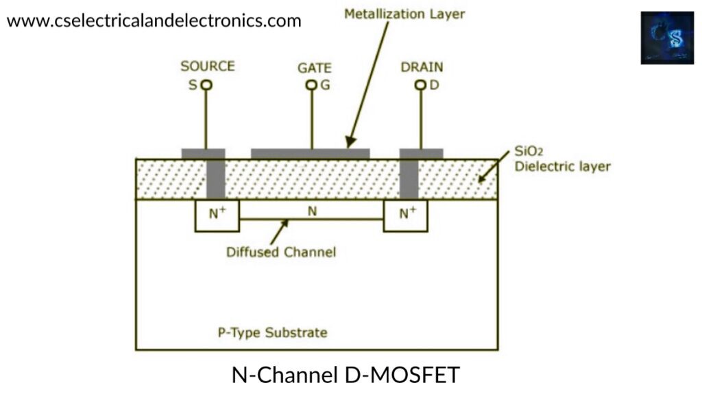
- N-channel D-MOSFET consists of two highly doped n regions that are diffused into lightly doped p-type substrate.
- The highly doped n regions represent the source and drain, which are connected through the metallic Contacts. The gate terminal is also connected to metal contact, but it remains insulated from the n channel by a thin layer of Silicon dioxide. There will be no direct electrical connection between the gate and the channel of MOSFET.
Operation Of N-Channel Depletion Type MOSFET
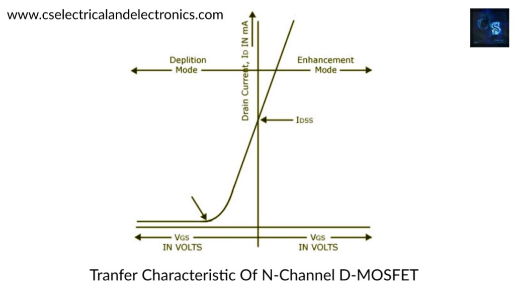
When the positive terminal is connected to the gate. The positive charge attracts the electrons towards the gate. This establishes current through the channel and it will be denoted by Idss. When we apply negative gate voltage, the negative charges which will be present on the gate terminal will repel conduction electrons from the channel and attract holes (positively charged) from the P-type substrate.
This will initiate the recombination of electrons and holes, and this will depend on the magnitude of the negative voltage applied to the gate terminal. The recombination reduces the number of electrons for conduction and reduces the drain current(Id). Due to recombination, the n channel is depleted and it decreases the conductivity of the channel. Higher the negative voltage, then higher will be the depletion of n-channel electrons. The level of drain current will decrease with the increase of negative bias for Vgs. For all positive values of Vgs, the positive gate will draw additional electrons from the P-type substrate due to reverse leakage current. Due to this, the Vgs increases, then Id also increases.
The application of a positive gate to source voltage has “enhanced” the level of free carriers in the channel to the encountered gate to source voltage is 0. Because of this reason, the region of positive gate voltages on the drain is called an enhancement region. The region between cut-off and saturation levels of Idss is called the depletion region.
P-Channel D-Mosfet
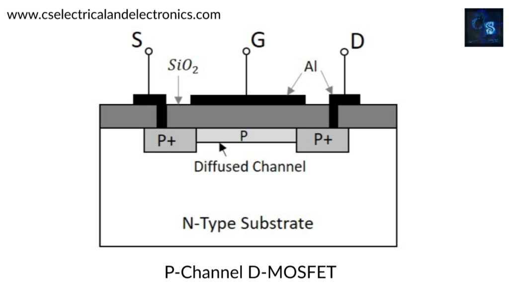
- The construction of the p-channel depletion type MOSFET will be completely opposite to that of n-channel depletion type MOSFET.
- Here, the substrate is n-type and the region channel is of P types. Then the polarities of voltage and the direction of the current are reversed. The drain characters look exactly similar to that of n- channel depletion type MOSFET. But Vds with negative values, Id is in the opposite direction and Vgs is having opposite polarities.
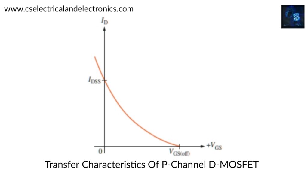
- The below graph shows the transfer characteristics of the p-channel depletion type MOSFET. Here, the transfer characteristics are a mirror image of the ID axis( vertical axis) of the transfer characteristic of n-channel depletion type MOSFET. Since the region is positive in the channel depletion region.
Enhancement MOSFET (E-MOSFET)
Most MOSFET operates only on the enhancement mode and it has no depletion mode. The depletion type MOSFET and enhancement type MOSFET is different i.e. it is not having a physical channel.
Construction of N-Channel E-MOSFET
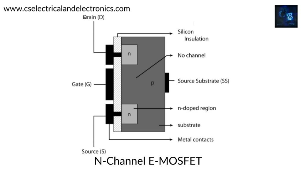
- N-channel E-mosfet consists of two highly doped n-regions, that are diffused into lightly doped P-type substrate. The source and drain terminals are taken out through metallic contacts.
- The channel between two n-regions will be absent in enhancement type mosfet. The silicon dioxide layer will be present to isolate the gate metallic platform from the region between a section of p-type material.
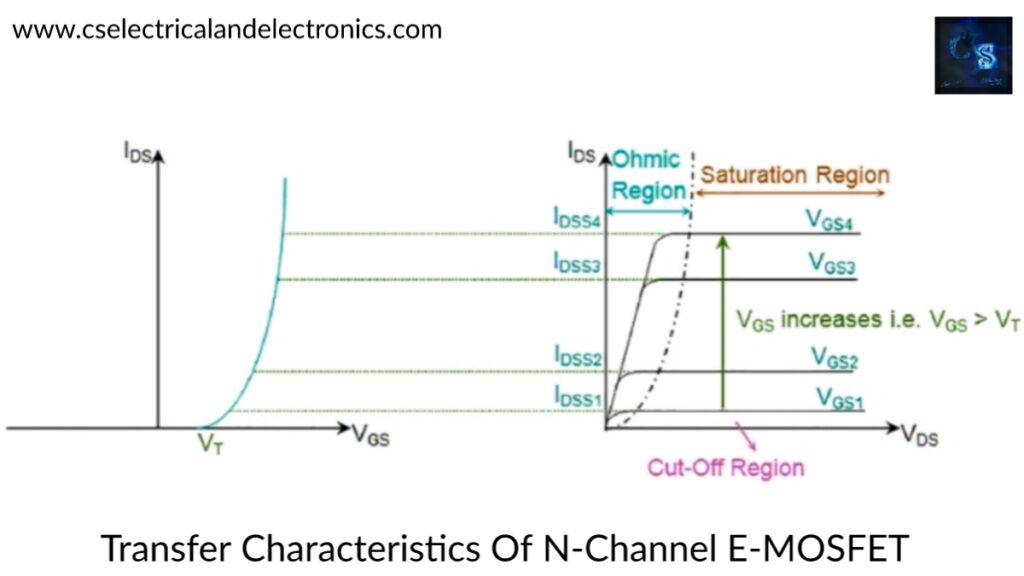
Operation Of Enhancement MOSFET
- On the application of drain to source voltage and gate to source, voltage is 0, by connecting the gate terminal directly to the source terminal.The zero current flows quite different from the depletion MOSFET.
- If you increase the magnitude of Vgs in the positive direction, then the concentration of electrons near the silicon dioxide layer increases.
- At a particular value of Vgs, some amount of current will flow between drain and source. The value at which current flows are called threshold voltage and it is denoted by Vt.
- In enhancement type n-channel mosfet a positive gate voltage above a threshold value induces a channel and drain current by creating a layer of negative charges adjacent to the SiO2 layer.
- The conductivity of the channel can be enhanced by increasing the gate to source voltage. The voltage which will be below the threshold value then there will be no channel. The channel will not exist with the value Vgs=0v and “enhanced” by the application of a positive gate to source voltage. This type of MOSFET can be called as enhancement type MOSFET.
Construction of P-Channel E-MOSFET
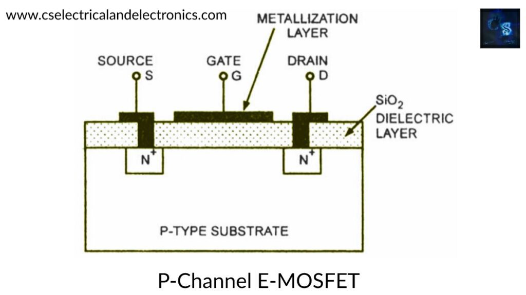
- The construction of the p-channel depletion type mosfet will be completely opposite to that of n-channel depletion type mosfet.
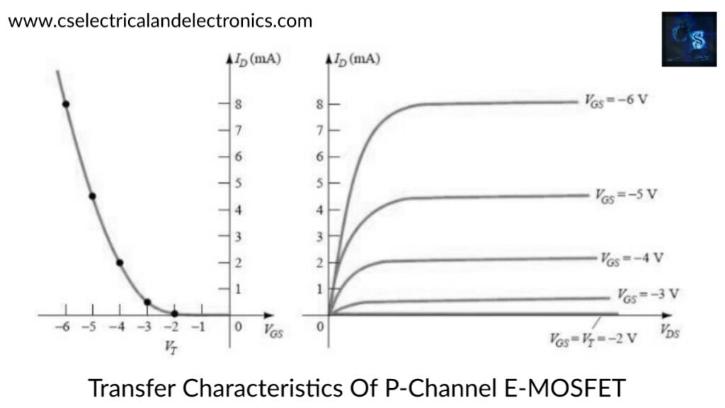
- Here, the substrate is n-type and regions, the channel is of P types. The polarities of the old age and the direction of the current are reversed. The drain characteristic for the p- channel enhancement type of mosfet appears exactly the same as p-channel d-mosfet, but with Vds negative and Id in the opposite direction and Vgs is having opposite polarities.
- The below graph shows the transfer characteristics of the p-channel depletion type mosfet. Here, the transfer characteristics is a mirror image about the ID axis( vertical axis) of the transfer characteristic of n-channel depletion type mosfet since the gate to source voltage is negative.
Applications Of MOSFET
- Used in switching and amplifying electronic signals.
- Used in designing of high-density VLSI techniques.
- Used in auto intensity control of street lights.
- Regulation of DC motors by power MOSFET.
Advantages Of MOSFET
- It provides greater efficiency when operating at lower voltages.
- Absence of gate current results in high input impedance, that produces high switching speed.
- Draws less current.
Disadvantages Of MOSFET
- Overload voltages make MOSFET as unstable.
- By using this oxide layer, it makes MOSFET vulnerable.
I hope this article may help you all a lot. Thank you for reading.
- 10 Free ADAS Projects With Source Code And Documentation – Learn & Build Today
- 100 + Electrical Engineering Projects For Students, Engineers
- 100+ Indian Startups & What They Are Building
- 1000+ Automotive Interview Questions With Answers
- 1000+ Electronics Projects For Engineers, Diploma, MTech Students
- 1000+ MATLAB Simulink Projects For MTech, Engineering Students
- 2000+ Embedded Systems Interview Question Bank
- 2026 Hackathons That Can Change Your Tech Career Forever