Hello guys, welcome back to our blog. Here in this article, we will discuss what parasitic capacitance and inductance are, how parasitic capacitance and inductance are caused, and the prevention of parasitic capacitance and inductance.
If you have any electrical, electronics, or computer science doubts, then ask questions. You can also catch me on Instagram – CS Electrical & Electronics.
Also, read the following:
- What Is Electric Highway, Countries Working On Electric Highway
- What Is ASIL A B C D, Purpose, Applications, Working, Examples
- What Is SoH In Battery, State Of Health, Methods, Purpose
Parasitic Capacitance And Inductance
A PCB is made up of several parallel wires, or traces, that are spaced apart by insulators. These traces create a capacitor with the help of dielectric material, which causes an undesired parasitic capacitance or stray capacitance effect.
There may be parasitic capacitance, parasitic resistance, or parasitic inductance in a PCB. When traces are tightly spaced, the parasitic capacitance effect is noticeable in high-frequency boards. The device’s operation is impacted by this utterly undesirable effect. It causes issues with signal integrity, EMI, and crosstalk. When creating the PCB layout, PCB designers that work with high-frequency, high data rates, and mixed-signal boards must take parasitic capacitance and inductance effects into account.
Parasitic Capacitance And Inductance In-Circuit Board
In all practical electronic devices, parasitic inductance—an undesirable inductance effect—is unavoidably present. Parasitic inductance, as opposed to intentional inductance, which is inserted into the circuit by using an inductor, is usually invariably an undesirable result. There are a select few applications, such as filters made of helical resonators, where parasitic inductance is really required. Capacitors show this effect much like any other genuine materials used in electronics, including resistors or even connecting wires.

In high-speed design, power electronics, and even multi-board power systems or systems with high-strength wireless capabilities, parasitic inductance is frequently treated as an afterthought. Any semiconducting or conducting structure on a PCB will have some parasitic inductance, which can cause issues like crosstalk, induced currents from electromagnetic interference (EMI), noise coupling, and other factors that reduce the quality of the signal.
Unfortunately, a PCB will always contain parasitic capacitance and inductance. A PCB is made up of several parallel conducting components that are spaced apart by insulators, essentially creating a capacitor. Similar to how conductors on a PCB always create complete loops, an equivalent inductor is produced.
It is quite challenging to measure the parasitic capacitance and inductance in a PCB. But it is immediately calculable from the ground up. Typically, you’ll find that parasitic capacitance is on the order of pF, whereas parasitic inductance is on the order of nH in various locations on your board. The parasitic capacitance and inductance on very large boards with longer and/or wider traces can be significantly larger.
Circuit board issues with digital and analog devices
Every pad and every trace on your board add their own parasitic capacitance and inductance, respectively. IR losses may also result from the parasitic resistance that pads add, albeit this can be reduced by using correct soldering techniques.
When working with any components that switch quickly, notably switching power supply, a voltage spike will be caused on a neighboring trace by the sudden burst of current from the switching component and the signal that is traveling along a trace. A higher induced voltage spike will occur on a trace with a larger parasitic inductance. In power electronics, however, this can result in unintentional switching in surrounding logic circuits, which generally raises bit error rates in digital systems.
In addition to increasing switching losses, parasitic capacitance in power electronics can prolong the switching time of high-speed FETs. The powerful magnetic fields produced during switching can still result in involuntary switching, even though this slightly lessens the resultant voltage spike in downstream components.
High-frequency analog signals can cause stray currents in analog circuits that can disrupt the operation of other analog components or the analog portion of a mixed signal component. When the parasitic inductance is as low as 1 nH, the analog signal from one trace or component might cause a low-level oscillation in another trace or component. Crosstalk is another effect of parasitic capacitance, and even small amounts of it can have an impact on an amplifier circuit’s gain.
Parasitic Capacitance and Inductance Reduction
Unfortunately, parasites can never be entirely eradicated. However, there are a few straightforward style decisions you may make to lessen parasite-related issues. Additionally, parasitic capacitance and inductance can cause signal issues, which can be avoided by choosing the appropriate components.
Making the equivalent loop area covered by traces as minimal as feasible is necessary to reduce parasitic inductance. The ground plane for essential traces should be positioned precisely above the layer holding your ground plane in order to do this. You can route some sensitive traces between the power and ground planes on a 4-layer board by placing the power plane on the bottom layer. As a result, signals in one layer won’t cause noise in signals in another layer due to EMI.
Thicker layers in your layer stack will result in a reduction in loop area and parasitic inductance, but thicker layers will result in an increase in parasitic capacitance. Therefore, the sweet spot where inductance is reduced and capacitance is increased is necessary. To find the ideal layer thickness, you may either manually compute this sweet spot or use simulation tools with various layer stacks. If you use a board with many layers, the layer thickness may occasionally be limited.
Parasitic capacitance and inductance can cause impedance mismatch throughout the signal channel in more recent high-speed digital applications where many data lines can operate at speeds of up to 10 Gbps. Any parasitic mismatch will result in reflections somewhere along the line, ultimately causing timing jitter and bit error rates to increase. The high-speed data signal cables should all have identical impedance.
You can apply the optimal layout options and lessen issues brought on by parasitic capacitance and inductance by using the appropriate design tools. You can find impedance mismatches that can result from parasitics with the aid of a design package that incorporates simulation capabilities. Additionally, you can experiment with various layout choices to lessen the impact of parasitics on the integrity of the signal.
To ensure that your design workflow is not interrupted and that your designs still keep their integrity when they are shipped out for production, it is a blessing that Cadence is offering the appropriate layout and design software with conveniently integrated analysis and simulation capabilities.
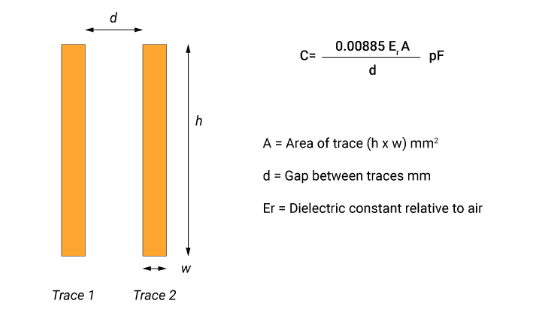
The calculation of parasitic capacitance
The conductors have an inherent quality called parasitic capacitance. It is the storing of changes in electric potential per unit of time. The formula for the parasitic capacitance is C=q/v. v is the voltage in volts, q is the charge in coulombs, and C is the capacitance in farads.
- Since there is no change in the potential for a constant electrical signal that does not fluctuate over time, dv/dt = 0, I = 0.
- If a capacitor is included in the circuit loop, dv/dt will converge to a fixed value, causing a change in potential and current flow; as a result, I not equal to 0.
C=(kA/11.3d)pF calculates the capacitance of a parallel plate capacitor. The relative dielectric constant of the board material, k, the plate area in cm2, the distance between the plates in cm, and the capacitance, C, are all given.
This was about “Parasitic Capacitance And Inductance“. I hope this article may help you all a lot. Thank you for reading.
Also, read:
- 10 Tips To Maintain Battery For Long Life, Battery Maintainance
- 10 Tips To Save Electricity Bills, Save Money By Saving Electricity
- 100 (AI) Artificial Intelligence Applications In The Automotive Industry
- 100 + Electrical Engineering Projects For Students, Engineers
- 100+ Indian Startups & What They Are Building
- 1000+ Automotive Interview Questions With Answers
- 1000+ MATLAB Simulink Projects For MTech, Engineering Students
- 2024 Is About To End, Let’s Recall Electric Vehicles Launched In 2024