
The global semiconductor industry is undergoing one of the most transformative phases in its history. As chips become the backbone of artificial intelligence (AI), 5G connectivity, automotive intelligence, edge computing, and next-generation consumer devices, the race to build smaller, faster, and more efficient processors has intensified. At the center of this technological revolution lies the transition to advanced process nodes like 3nm and now 2nm.
In this high-stakes global race, India has traditionally been seen as a strong design and software hub but not necessarily the epicenter of bleeding-edge chip innovation. That narrative is rapidly changing.
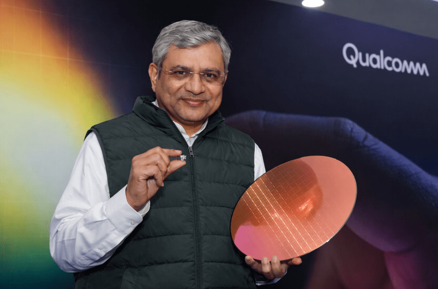
With Qualcomm’s India engineering teams contributing to the design and tape-out of a 2nm chip, the country is no longer just supporting global semiconductor innovation — it is actively shaping it. From Bengaluru’s thriving tech ecosystem to Hyderabad and Chennai’s growing semiconductor clusters, Indian engineers are now playing a central role in building next-generation chips that will power billions of devices worldwide.
This article explores how India — particularly through Qualcomm’s engineering presence — is shaping the future of 2nm chip design, why this milestone matters globally, and what it means for AI, automotive, and the broader semiconductor ecosystem.
Understanding 2nm: More Than Just a Number
Before diving into India’s role, it’s important to understand what 2nm represents.
In semiconductor manufacturing, “2nm” refers to a process node generation. Historically, node names corresponded roughly to physical transistor gate lengths. Today, however, 2nm is more of a generational benchmark representing:
- Higher transistor density
- Improved performance per watt
- Advanced transistor architectures
- More complex design rules
- Greater power efficiency
At 2nm, chips typically move toward Gate-All-Around (GAA) transistor architectures, replacing earlier FinFET designs. GAA allows better electrostatic control, reduced leakage, and improved performance — all critical for AI and high-performance computing.
The smaller the node, the greater the engineering complexity. Design challenges grow exponentially due to:
- Increased variability
- Tighter layout constraints
- Advanced lithography requirements
- Complex power integrity considerations
- Thermal management issues
Successfully taping out a 2nm chip design is not just incremental progress — it’s a declaration of engineering maturity.
Qualcomm in India: From Support Center to Innovation Hub
Qualcomm’s presence in India spans over two decades. What started as a strategic engineering extension has evolved into one of Qualcomm’s largest R&D hubs outside the United States.
Today, Qualcomm’s India centers — particularly in:
- Bengaluru
- Hyderabad
- Chennai
- Noida
— contribute across the entire chip development lifecycle:
- Architecture exploration
- RTL design
- Physical design
- Verification and validation
- AI software optimization
- System integration
- Post-silicon testing
The successful 2nm tape-out milestone demonstrates that Indian teams are not just executing tasks — they are leading complex, cutting-edge development initiatives.
Bengaluru: The Semiconductor Brain Hub
Bengaluru, often called India’s Silicon Valley, has become a major global center for semiconductor design. The ecosystem includes:
- Multinational semiconductor companies
- EDA tool providers
- AI startups
- Automotive technology firms
- Research institutions
Qualcomm’s Bengaluru facility has grown into a critical innovation engine. Engineers here work on:
- Advanced SoC (System-on-Chip) integration
- AI accelerators
- Modem technologies
- Low-power architecture design
- 5G and future 6G research
The 2nm design milestone emerging from this ecosystem highlights how India’s semiconductor talent has matured from backend execution to architectural leadership.
What “Tape-Out” Really Means
In semiconductor design, “tape-out” marks the moment when the final chip design is sent to the foundry for fabrication.
This is not a trivial event. Tape-out represents:
- Completion of design verification
- Final sign-off on timing, power, and physical layout
- Resolution of DRC (Design Rule Check) and LVS (Layout vs. Schematic) issues
- Confidence in manufacturability
At 2nm, achieving tape-out is exponentially harder due to:
- Advanced EUV lithography constraints
- Multi-patterning challenges
- Complex power delivery networks
- Tighter reliability margins
For India-based teams to contribute to a 2nm tape-out signals deep expertise in advanced node physical design, verification, and system integration.
Why 2nm Matters for AI
Artificial intelligence workloads are reshaping chip architecture.
AI requires:
- Massive parallelism
- High memory bandwidth
- Low latency
- Energy efficiency
Smaller nodes like 2nm enable:
- Higher transistor density for AI accelerators
- Improved TOPS per watt (Tera Operations Per Second per watt)
- Better integration of CPU, GPU, NPU, and modem components
- Advanced on-device AI capabilities
Qualcomm’s focus on AI-enabled Snapdragon platforms aligns perfectly with 2nm’s advantages. Indian engineers working on AI optimization and hardware-software co-design play a pivotal role in this transformation.
The Shift to Gate-All-Around (GAA)
One of the defining characteristics of the 2nm generation is the transition from FinFET to Gate-All-Around transistor architectures.
GAA provides:
- Better channel control
- Reduced leakage current
- Improved scalability
- Enhanced power efficiency
However, designing for GAA introduces new challenges:
- New layout rules
- Complex parasitic extraction
- Updated EDA tool flows
- More stringent timing closure
Indian engineers contributing at this level must deeply understand device physics, physical design constraints, and power-performance-area (PPA) trade-offs.
India’s Talent Advantage
India hosts an estimated 20% of the world’s semiconductor design engineers. This concentration of talent offers several advantages:
- Strong mathematical and engineering foundations
- Cost-effective R&D scaling
- Rapid learning curve in emerging technologies
- Experience across global semiconductor projects
But beyond numbers, the real shift lies in capability maturity. Indian teams now:
- Lead complex IP integration
- Drive AI acceleration research
- Contribute to next-gen wireless standards
- Work on system-level optimization
The 2nm milestone reflects years of accumulated experience across 7nm, 5nm, and 3nm generations.
AI + Semiconductor Co-Design: The New Engineering Paradigm
Modern chip development is no longer just about transistor scaling. It is about system-level intelligence.
Qualcomm’s future strategy revolves around:
- Edge AI
- Automotive intelligence
- Extended reality (XR)
- IoT and connected devices
India-based engineers increasingly work at the intersection of:
- Hardware architecture
- AI model optimization
- Compiler stacks
- Power management
- Security frameworks
This hardware-software co-design approach is essential at 2nm, where power and thermal budgets are tight.
Automotive and 2nm: A Strategic Alignment
The automotive industry is undergoing digital transformation:
- ADAS (Advanced Driver Assistance Systems)
- Autonomous driving
- In-vehicle infotainment
- Digital cockpits
- Software-defined vehicles (SDVs)
These systems require:
- High compute density
- Real-time AI processing
- Functional safety compliance
- Low power consumption
2nm nodes provide performance headroom while maintaining energy efficiency — critical for electric vehicles.
Qualcomm’s automotive platforms benefit directly from advanced node scaling, and India’s engineering ecosystem — already strong in automotive embedded systems — aligns naturally with this direction.
India Semiconductor Mission: Policy Meets Capability
India’s government has launched initiatives like the India Semiconductor Mission (ISM) to:
- Strengthen chip design ecosystems
- Promote semiconductor manufacturing
- Encourage talent development
- Attract global partnerships
The 2nm milestone reinforces the argument that India is ready for deeper participation in the global semiconductor value chain.
Design leadership often precedes manufacturing investment. As India proves its advanced-node capabilities, it strengthens its case for attracting foundry ecosystems and advanced packaging facilities.
The Global Competitive Landscape
The 2nm race includes:
- TSMC
- Samsung
- Intel
Design companies like Qualcomm, Apple, Nvidia, and AMD rely on these foundries for manufacturing.
While fabrication may happen abroad, chip design excellence determines product competitiveness. India’s growing role in design means it is becoming strategically relevant in global semiconductor geopolitics.
Challenges of Designing at 2nm
Despite the milestone, challenges remain:
- Rising design costs
- Tool complexity
- Thermal density issues
- Reliability concerns
- Supply chain dependencies
Advanced node design can cost hundreds of millions of dollars. It requires robust EDA ecosystems, cross-functional collaboration, and continuous upskilling.
India must continue investing in:
- Advanced semiconductor education
- Device physics research
- EDA tool development
- Packaging innovation
Skill Evolution in Indian Semiconductor Engineers
The 2nm era demands new skills:
- Advanced physical design methodologies
- Low-power architecture expertise
- AI hardware acceleration
- Advanced verification techniques
- Cross-domain system thinking
Indian engineers are increasingly gaining exposure to:
- Multi-die packaging
- Chiplet architectures
- Heterogeneous integration
- Advanced reliability modeling
This skill evolution is critical for sustaining leadership at future nodes like 1.8nm and beyond.
From Execution to Ownership
A decade ago, many semiconductor tasks outsourced to India were limited in scope.
Today, Indian teams:
- Own critical IP blocks
- Lead subsystem development
- Drive innovation roadmaps
- Collaborate directly with global architecture teams
The 2nm tape-out represents symbolic and practical proof of this ownership shift.
Edge AI and India’s Strategic Role
Edge AI is one of Qualcomm’s strongest focus areas.
2nm enables:
- On-device large language model acceleration
- Real-time vision processing
- AI-powered cameras
- Smart IoT ecosystems
Indian engineers working on AI stack optimization help ensure these chips deliver real-world intelligence efficiently.
As AI becomes embedded everywhere — from smartphones to vehicles — India’s contribution grows exponentially in importance.
Economic and Strategic Implications
The semiconductor industry drives:
- National security
- Digital infrastructure
- Economic growth
- Technological sovereignty
India’s involvement in 2nm design strengthens:
- Global credibility
- Talent export value
- Domestic semiconductor ambitions
- Startup ecosystem growth
It also signals to global investors that India is capable of advanced engineering leadership.
The Road Ahead: Beyond 2nm
The industry is already discussing:
- 1.8nm
- 1.4nm
- Advanced 3D stacking
- Chiplet-based architectures
Future progress may depend more on:
- Packaging innovation
- AI-driven design automation
- Energy efficiency breakthroughs
India’s ability to stay at the forefront will depend on sustained investment in research, academia-industry collaboration, and talent upskilling.
Conclusion: A Defining Shift in India’s Semiconductor Identity
The story of Qualcomm’s 2nm milestone is not just about a chip. It represents a deeper transformation in India’s role within the global semiconductor ecosystem.
From Bengaluru’s dynamic engineering hubs to cross-functional AI and hardware co-design teams, Indian engineers are now shaping technologies that will define the next decade of computing.
2nm is not merely a number. It is a symbol:
- Of engineering maturity
- Of global competitiveness
- Of AI-driven innovation
- Of India’s transition from participant to leader
As chips become the foundation of AI, autonomous systems, and connected intelligence, India’s role will only expand.
From Bengaluru to 2nm, the journey is just beginning — and the future of semiconductor innovation will increasingly carry India’s signature.
Thanks for reading.
Also, read:
- India’s GaN Chip Breakthrough: Why Gallium Nitride Could Shape the Future of Defense Electronics
- India’s Chip Era Begins: A New Chapter in Semiconductor Manufacturing
- FlexRay Protocol – Deep Visual Technical Guide
- Top 50 AI-Based Projects for Electronics Engineers
- India AI Impact Summit 2026: The Shift from AI Hype to AI Utility
- Python Isn’t Running Your AI — C++ and CUDA Are!
- UDS (Unified Diagnostic Services) — Deep Visual Technical Guide
- Automotive Ethernet — Deep Visual Technical Guide