Hello guys, welcome back to my blog! ♻️?
Today, we’re exploring one of the most groundbreaking innovations in electronics — the fully recyclable 3D-printed PCBs that are transforming prototyping and reducing e-waste. From sustainable materials to cutting-edge manufacturing methods, this new technology is making electronics greener and more accessible than ever before.
In this article, I’ll introduce you to DissolvPCB — a revolutionary approach that uses water-soluble substrates and liquid metal conductors to create eco-friendly circuit boards. You’ll learn how this technology is helping researchers, makers, and engineers quickly prototype designs while cutting down on waste, cost, and environmental impact.
Ask questions if you have any electrical, electronics, or computer science doubts. You can also catch me on Instagram – CS Electrical & Electronics.
- Top 30 YouTube Tutorials Every Automotive Engineer Must Watch in 2025
- Vikram-32 (Vikram-3201) — India’s First Indigenous 32-bit Space-Grade Processor
- Ather’s 2025 Innovations: The Complete Guide To Smarter, Safer, And Futuristic Electric Scooters
How PVA and Liquid Metal Are Revolutionizing PCB Prototyping And E-Waste Management
Before diving into the technology itself, it’s important to understand what PCBs are and why they’re crucial to electronics. At their core, PCBs are the backbone of almost every electronic device you use — from smartphones and laptops to electric vehicles and medical devices.
✅ 1. What Are Printed Circuit Boards (PCBs)?
A PCB mechanically supports and electrically connects electronic components using conductive tracks, pads, and pathways etched from copper sheets laminated onto a non-conductive substrate. These boards serve as platforms for mounting resistors, capacitors, microchips, and more, allowing signals and power to flow through complex circuits.
Traditional PCBs are typically made from FR-4, a composite material consisting of woven glass fiber and epoxy resin. While FR-4 is durable and efficient, it presents several environmental and manufacturing challenges.
✅ 2. The Problem with Traditional PCBs
While traditional PCBs have powered the electronics revolution, they come with significant downsides:
? E-Waste Crisis
The electronics industry is one of the largest contributors to global waste, with millions of tons of discarded devices and components accumulating every year. Recycling PCBs is difficult because they’re made from complex materials bonded tightly together, making separation challenging.
? Hazardous Materials
PCBs often contain lead, brominated flame retardants, and other chemicals that are harmful to both the environment and human health if not properly processed.
? Complex Recycling
The separation of copper, fiberglass, and epoxy requires energy-intensive processes or produces toxic byproducts. In many parts of the world, discarded PCBs are burned or buried, leading to soil and water contamination.
? Cost and Resource Intensity
Traditional recycling methods are expensive and inefficient, and the extraction of copper and other metals continues to put pressure on global resources.
With the increasing demand for electronics, especially in fields like electric vehicles, IoT, and renewable energy, the need for sustainable alternatives is greater than ever.
✅ 3. Introducing DissolvPCB – A Sustainable Innovation
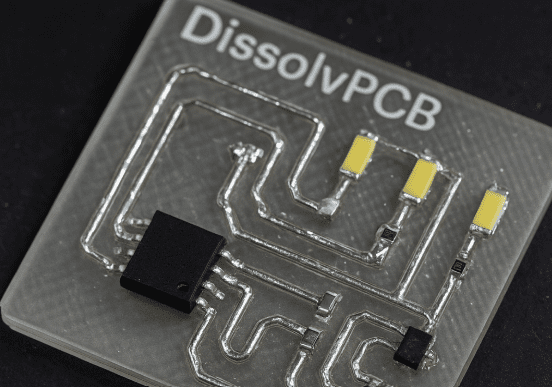
Researchers from the University of Maryland, Georgia Tech, and the University of Notre Dame have introduced a game-changing solution — DissolvPCB. This fully recyclable 3D-printed PCB combines materials that are eco-friendly and easily recoverable, offering an elegant alternative to traditional designs.
The key to this innovation lies in two materials:
- Polyvinyl Alcohol (PVA): A water-soluble polymer used as the substrate.
- Eutectic Gallium-Indium (EGaIn): A liquid metal alloy that remains conductive while being easily recoverable after dissolution.
This combination allows the PCB to be printed using standard 3D printing techniques and then dissolved in water after use, enabling almost complete recovery of the materials without the need for complex separation processes.
✅ 4. How Does DissolvPCB Work?
? Materials Used
- PVA (Polyvinyl Alcohol):
PVA is a biodegradable and water-soluble material that forms the base of the PCB. Unlike traditional fiberglass-epoxy composites, it dissolves easily in water without leaving harmful residues. - EGaIn (Eutectic Gallium-Indium):
EGaIn is a liquid metal alloy that remains conductive while being non-toxic and recyclable. It replaces copper pathways, allowing for flexible and corrosion-resistant circuits.
? The Manufacturing Process
- 3D Printing:
Using conventional 3D printers, PVA forms the structure of the PCB while channels are filled with liquid metal EGaIn to create conductive pathways. - Component Mounting:
Both through-hole and surface-mounted components can be attached easily, making the board compatible with a wide range of electronics. - Testing and Prototyping:
Once assembled, the board performs like a conventional PCB, supporting current flow and signal transmission at high frequencies.
? Dissolution and Recovery
After testing or prototyping is complete, the board is simply immersed in water. The PVA substrate dissolves fully, separating the liquid metal from the structure. The recovery rates are remarkable:
- PVA: 99.4% recovery
- EGaIn: 98.6% recovery
This process allows both materials to be reused for new boards, reducing cost and waste dramatically.
✅ 5. Performance and Applications
? High-Current and High-Frequency Capabilities
One might think that eco-friendly PCBs would compromise on performance — but that’s not the case. DissolvPCB can support:
- Current loads up to 5A, suitable for many power applications.
- Signal frequencies up to 10 MHz, making it viable for communication systems and control circuits.
? Prototyping & Experimentation
The ability to dissolve and reuse the board makes it perfect for research labs, universities, and makerspaces where designs are constantly evolving. Engineers can print, test, dissolve, and reprint boards without the overhead of sourcing new materials.
? Compatibility with Modern Electronics
DissolvPCB is designed to support both through-hole and surface-mounted devices (SMDs), making it adaptable to existing electronic designs. A FreeCAD plugin also assists in converting KiCad files for quick fabrication.
✅ 6. Environmental Impact
? Reducing E-Waste
By providing a circular lifecycle — print, test, dissolve, and reuse — DissolvPCB dramatically reduces the volume of discarded electronics, especially in prototyping environments.
? Efficient Recycling
Unlike traditional PCBs, which require chemical or thermal processes for recycling, DissolvPCB’s materials can be recovered with minimal energy input, making the process both efficient and sustainable.
? Comparison with FR-4 Boards
| Feature | Traditional FR-4 PCBs | DissolvPCB |
|---|---|---|
| Recycling method | Complex & hazardous | Simple water-based |
| Recovery rates | Low, inefficient | Up to 99.4% PVA & 98.6% EGaIn |
| Environmental impact | High waste & pollution | Minimal waste, eco-friendly |
| Manufacturing cost | Higher due to complex processes | Lower due to reuse |
✅ 7. Challenges and Limitations
While promising, DissolvPCB is not without its challenges:
? Durability Concerns
Water-soluble substrates are ideal for temporary use, but they may not withstand long-term exposure to humidity or physical stress.
? Industrial Scale
Though perfect for prototyping, large-scale production and consumer electronics may require further research to improve longevity and robustness.
? Cost and Accessibility
Liquid metals like EGaIn are more expensive than copper, and not all labs or manufacturers are equipped for this type of fabrication.
✅ 8. Future Prospects
? Advanced Prototyping
Startups, universities, and research centers are likely to adopt this technology for cost-effective experimentation.
? Educational Tools
Schools and training centers can use DissolvPCB for hands-on electronics learning, reducing waste from failed experiments.
? Consumer Electronics
As material costs drop and durability improves, recyclable PCBs could find their way into niche markets such as eco-friendly wearables or temporary electronics.
✅ 9. How You Can Get Started
If you’re eager to explore DissolvPCB technology, here’s how you can begin:
- Research Materials: Look into suppliers of PVA filaments and EGaIn alloys.
- Use Open-Source Tools: FreeCAD plugins and KiCad files can help you design circuits for 3D printing.
- Start Small: Experiment with low-power prototypes and simple circuits before expanding.
- Connect with Communities: Join electronics and sustainability forums to share designs and ideas.
- Stay Updated: Follow research from universities and industry publications on recyclable electronics.
✅ 10. Final Thoughts
DissolvPCB is a shining example of how technology and sustainability can go hand-in-hand. By rethinking how circuit boards are designed, used, and recycled, this innovation is helping the electronics industry tackle the mounting challenges of e-waste and resource scarcity.
While it may not yet be a replacement for consumer electronics, its potential for research, prototyping, and education is enormous. As the world shifts toward greener practices, eco-friendly electronics like DissolvPCB will play an increasingly important role.
Whether you’re an engineer, student, or electronics hobbyist, embracing these sustainable practices today can set the stage for smarter and cleaner innovation tomorrow.
Let’s build a future where technology powers progress — without costing the planet. ?⚙️?
This was about “How PVA and Liquid Metal Are Revolutionizing PCB Prototyping And E-Waste Management“. Thank you for reading.
- NVIDIA RTX Spark And The Reinvention Of Personal Computing In The AI Era
- Create Simulink Models With AI In Just 2 Minutes
- Tata Electronics Signs a Game-Changing Agreement with Dutch Semiconductor Giant ASML
- Best Onsite Countries For Indians In 2026 – Complete Guide for Embedded Engineers
- RTOS Concepts Explained Visually
- Classic And Adaptive AUTOSAR Explained Visually
- ASPICE Tutorial Explained Visually
- India’s 2nd Semiconductor Plant: How Kaynes Semicon Built It in Just 14 Months